-advertisement-
On May 31, 2024, the University of Tokyo announced that it had developed a technique for drilling ultra-fine holes in an intermediate substrate, known as a "package substrate," which connects semiconductor chips to printed circuit boards. This technology was developed in collaboration with Ajinomoto Fine-Techno, Mitsubishi Electric, and Spectronix under the "TACMI Consortium," established by the university as a venue for industry-academia-government collaboration. This processing technology allows for the creation of holes with a diameter of 3μm in the insulating layer on a glass substrate using only laser processing.
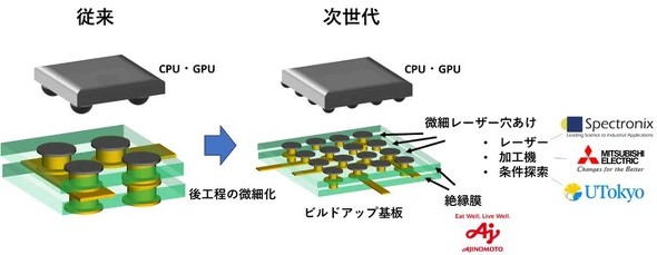
Overview of laser micro-hole drilling technology on semiconductor substrates [Source: The University of Tokyo]
Firstly, the University of Tokyo deposited copper on a glass substrate and then used laser processing to create fine copper wiring patterns by carving out the copper in a patterned manner. On top of this, Ajinomoto Fine-Techno layered the semiconductor interlayer insulating material "Ajinomoto Build-Up Film (ABF)" to a thickness of 3μm. The deep ultraviolet (DUV) high-power laser with a wavelength of 266nm used for drilling was provided by Spectronix, and Mitsubishi Electric improved the focusing size of the laser processing machine, making it smaller than before.
Based on condition exploration using AI (artificial intelligence) by the University of Tokyo, they irradiated the ABF with a DUV laser and successfully drilled holes with a diameter of 3μm at intervals of 5μm. When confirmed with a cross-sectional electron microscope photograph, the holes were found to be created only in the ABF, leaving the copper wiring and glass substrate intact.
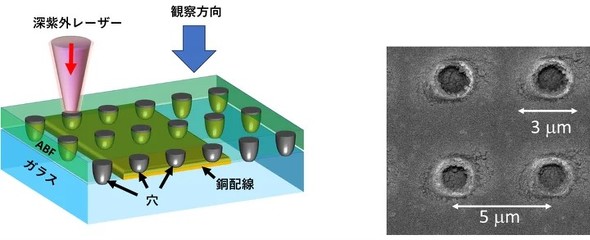
Electron microscope photograph of the created micro-holes viewed from above [Source: The University of Tokyo]
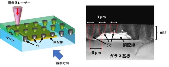
Cross-sectional electron microscope photograph of the created micro-holes [Source: The University of Tokyo]
Compared to conventional methods, the developed technology allows for drilling smaller holes. This enables higher density wiring and more flexible substrate processing in semiconductor chips, which are becoming increasingly miniaturized.
Moving forward, the four parties will continue to expand the range of laser processing applications and work towards industrial applications of this technology by engaging with semiconductor manufacturers.
Editor:Lulu
▼▼▼
Customs commissioner visits Simmtech to address import and export challenges
India's push to limit Chinese PCB imports faces resistance from automakers
Driven by the expansion of rigid PCB sales, BH will achieve strong medium to long-term growth
SKC aims for 10 trillion won in sales by 2027, driven by copper foil and glass substrates
Shin-Etsu Chemical develops semiconductor packaging substrate manufacturing equipment
KSG GmbH achieves remarkable energy efficiency milestone with sustainable innovations
+86 191 9627 2716
+86 181 7379 0595
8:30 a.m. to 5:30 p.m., Monday to Friday

