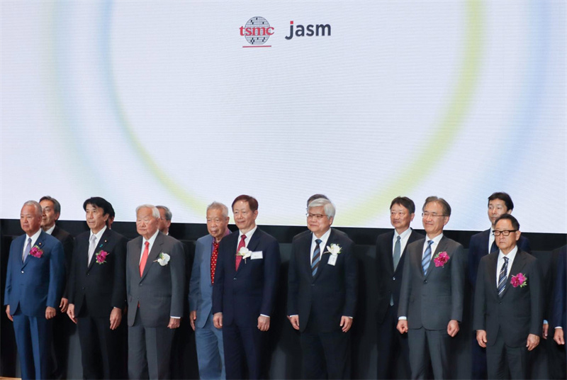
Japan's semiconductor industry has reached a significant milestone with the start of mass production at TSMC's first wafer fab in Kumamoto, operated by its subsidiary, Japan Advanced Semiconductor Manufacturing (JASM). This development, confirmed by Kumamoto Prefecture Governor Takashi Kimura on December 27, 2024, marks a major step in Japan's efforts to revitalize its semiconductor sector.
The announcement followed a notification from JASM to the local government on December 23, confirming that the Kumamoto fab had officially begun production. While the exact date of the commencement remains unclear, the local government has already mandated regular monitoring of the facility's wastewater emissions starting in January 2025. This move comes in response to local concerns regarding groundwater consumption and environmental impacts from wastewater discharge.
Key Investments and Production Plans
TSMC's Kumamoto wafer fab is part of a broader $8.27 billion initiative, supported by up to ¥476 billion ($3.3 billion) in subsidies from Japan's Ministry of Economy, Trade, and Industry (METI). This first fab will focus on producing logic chips, including 12/16nm and 22/28nm process technologies, for key clients Sony Semiconductor Solutions (SSS) and Denso. The plant aims to meet the increasing demand for image sensors and automotive semiconductors.
Construction on the fab began in April 2022, and it was completed by December 2023, featuring state-of-the-art facilities, including a 4.5-square-meter cleanroom.

Second and Future Expansion Plans
The second wafer fab in Kumamoto is set to begin construction in early 2025, with operations expected to start by 2027. This second facility will extend production capabilities to include 6/7nm process technologies, further expanding TSMC's footprint in Japan. When both fabs are fully operational, their combined production capacity will exceed 100,000 wafers per month.
Governor Kimura has expressed interest in bringing a third TSMC wafer fab to Kumamoto, but acknowledged that such a project remains uncertain and could take years to materialize. He emphasized that the success of the first two fabs would be critical to the decision, with ongoing efforts to address environmental concerns, traffic congestion, and the support of the local community.

Boosting Japan's Semiconductor Industry
This project represents a crucial part of Japan's strategy to revive its semiconductor industry, which has lagged behind global trends in recent decades. The Japanese government has committed significant resources to bolster the sector, offering subsidies and incentives to attract major players like TSMC. In particular, the government is focusing on the rapidly growing electric vehicle (EV) and AI markets, both of which rely heavily on advanced semiconductor technologies.
To support these efforts, JASM has already hired over 3,400 local employees and aims to source 60% of the semiconductor components for the Kumamoto fabs from local suppliers by 2030. Currently, over 45% of the materials come from Japan, with the goal of reaching 50% by 2026.
This ambitious plan not only strengthens Japan's semiconductor manufacturing capabilities but also aims to boost local supply chains and create thousands of high-tech jobs, positioning Kumamoto as a key player in the global semiconductor race.
+86 191 9627 2716
+86 181 7379 0595
8:30 a.m. to 5:30 p.m., Monday to Friday
