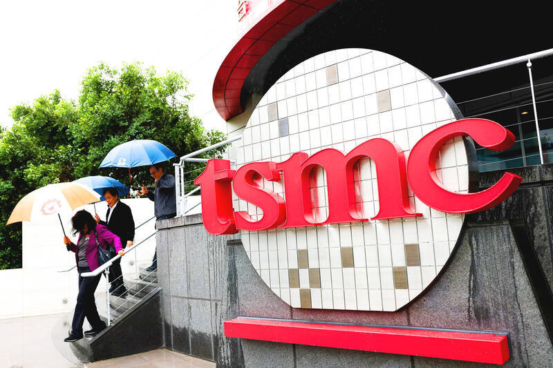
Taiwan Semiconductor Manufacturing Company (TSMC) continues to strengthen its position as a global leader in semiconductor technology with notable advancements across multiple fronts, including its next-generation 2nm process, cutting-edge silicon photonics strategy, and major fab expansions in Kaohsiung.
Progress in 2nm Technology
TSMC is making significant strides in its 2nm (N2) process, with plans for aggressive scaling of production. The company recently commenced setting up a pilot production line at its Hsinchu Baoshan fab (Fab 20), targeting a monthly capacity of 3,000 to 3,500 wafers. By the end of 2025, TSMC expects to ramp up its 2nm capacity to over 50,000 wafers per month, with further growth to 120,000 to 130,000 wafers per month by 2026. The company's Kaohsiung fab (Fab 22) will contribute significantly to this expansion, with a forecasted monthly output of 25,000 to 30,000 wafers by the end of 2025, growing to 60,000 to 65,000 by 2027.
TSMC's Chairman, C.C. Wei, emphasized that demand for 2nm technology surpasses that for the 3nm process, with major customers like Apple, MediaTek, Qualcomm, Intel, and NVIDIA poised to adopt this advanced technology. Additionally, TSMC's 2nm process is expected to offer up to 35% power reduction or a 15% performance boost at the same voltage, while transistor density will increase by 15% compared to the 3nm generation.
Pioneering Silicon Photonics
TSMC has also achieved a major milestone in its silicon photonics strategy. The company has successfully integrated co-packaged optics (CPO) with its advanced semiconductor packaging technologies, a breakthrough that paves the way for the 1.6T optical transmission era by 2025. TSMC's trial production of the micro ring modulator (MRM) using its 3nm process marks a significant step towards high-performance computing (HPC) and AI applications, with Broadcom and NVIDIA expected to be among the first customers.
Despite challenges in CPO module production, including low yield rates and the complex packaging process, TSMC is positioning itself to lead the way in optical signal transmission for computing tasks. The integration of CPO with advanced packaging solutions such as CoWoS or SoIC will eliminate the speed limitations of traditional copper interconnects, making TSMC’s silicon photonics technology critical for the next generation of HPC and AI chips.
Fab Expansions in Kaohsiung
In addition to advancing its semiconductor technologies, TSMC is expanding its manufacturing footprint with plans to build two new wafer fabs in Kaohsiung (P4 and P5) starting in 2026. These new fabs, part of a larger expansion plan in the region, will focus on developing high-end processes, including the 2nm technology that will drive TSMC’s future growth. Construction of these fabs will create around 8,000 new jobs and support the company’s goal of staying competitive in the fast-evolving global semiconductor market.

The first fab in Kaohsiung (P1) is set to begin mass production of 2nm chips next year, while P2 and P3 will also support this process by 2026. Notably, the 2nm process promises to deliver 10% to 15% better speed performance and consume less power than the enhanced 3nm (N3E) process, making it crucial for applications requiring high performance and energy efficiency, such as AI and advanced computing.

Looking Ahead: Growth and Global Competition
As TSMC continues its expansion and technology development, the company is poised to play a central role in meeting the surging global demand for AI chips. Analysts forecast that TSMC's revenue will grow by 20% next year, driven by increasing orders from clients like NVIDIA for their B200 and B300 AI chips. Despite potential challenges from global trade policies, including possible tariff hikes on US-bound goods, TSMC’s diversified production base and strong demand for its advanced semiconductor technologies should allow it to maintain its market leadership.
The company’s investor conference, scheduled for this January, is expected to shed light on its growth trajectory and strategies to address global semiconductor competition. As TSMC advances both its technology and production capacity, it is already shaping the semiconductor industry’s next wave of innovation.
+86 191 9627 2716
+86 181 7379 0595
8:30 a.m. to 5:30 p.m., Monday to Friday
