
-advertisement-
Mark Liu, chairman of TSMC, made a secret visit to the headquarters of ASML May this year. The visit aimed to discuss the purchase of next-generation extreme ultraviolet (EUV) lithography equipment, specifically the "High Numerical Aperture (NA EUV)" machines, which are crucial for advancing semiconductor manufacturing technology.
The Taiwanese daily United Daily News reported on July 18 that Mark Liu's visit to ASML nearly finalized the purchase of the NA EUV lithography equipment. This equipment is expected to be installed at TSMC's R&D center this fall and will be instrumental in the development of "A10 technology," which pertains to the next-generation 1nm process. This process represents a significant leap in semiconductor technology, enabling the production of smaller, more powerful, and more efficient chips.
During the same visit in May, Mark Liu also visited the German industrial laser company TRUMPF and postponed TSMC's Taipei technology symposium to accommodate these critical meetings. The discussions with ASML were pivotal, although sources indicated that TSMC and ASML failed to reach an agreement on the price of the NA EUV equipment. Despite this, there was a progress in relocating the R&D center from the Netherlands to Hsinchu, Taiwan, said industry sources.
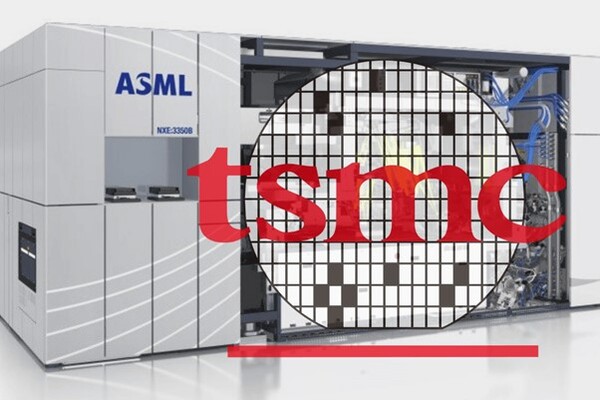
The semiconductor industry is highly globalized, with different stages of production often taking place in various countries. TSMC, as the world's largest semiconductor foundry, plays a crucial role in this supply chain, manufacturing advanced chips for major tech companies like Apple, AMD, and NVIDIA. ASML, a Dutch company, is the sole supplier of EUV lithography machines, which are essential for producing the most advanced semiconductor nodes.
EUV lithography technology is a cutting-edge method used to create very fine patterns on silicon wafers, enabling the production of smaller and more powerful semiconductor devices. The High Numerical Aperture (NA EUV) machines represent an advanced version of this technology, expected to further shrink chip sizes and increase their performance. The development of 1nm process technology, where the components on a chip are only one nanometer in size, marks a significant advancement from current technologies and is anticipated to lead to more powerful and efficient chips.
▼▼▼
Taiwan chip firm GlobalWafers wins $400m for US factories
AMD and IIT-B join hands to support semiconductor startups in India
MediaTek develops Arm-based server chips with TSMC's 3nm process
Cyient announces a dedicated semiconductor subsidiary
Accenture buys its second chip services firm in a week
+86 191 9627 2716
+86 181 7379 0595
8:30 a.m. to 5:30 p.m., Monday to Friday

