On February 27, TASMIT Inc. has introduced a cutting-edge inspection system for glass substrates as part of its INSPECTRA® series, renowned for its efficiency in advanced semiconductor manufacturing. This new system is designed to detect pattern defects, foreign particles, cracks, and other glass-specific flaws, and is compatible with glass core interposers and rewiring glass carriers used in panel level packaging (PLP) and high-density PCB manufacturing.
While previous systems could only inspect surface defects, TASMIT's innovation is the first in the industry capable of examining both front and back surfaces as well as the internal structure of glass substrates. This breakthrough is particularly significant for the PCB industry, where high-density packaging and advanced interposer technologies are driving the need for more precise and comprehensive defect detection.
The company targets advanced semiconductor manufacturers, particularly in PLP and PCB applications, aiming for 1 billion yen in orders by FY2025 and 2 billion yen by FY2030. The demand for larger semiconductor chips and higher integration in next-gen 2.5D packaging has necessitated larger interposers. Traditionally, silicon interposers from 12-inch wafers were used, but their circular shape limits chip yield. Glass substrates, which can be manufactured in larger sizes and are ideal for high-density packaging, are emerging as a viable alternative. TASMIT's system supports industry-standard 650mm square glass substrates, making it a game-changer for PCB manufacturers seeking to enhance production efficiency and yield.
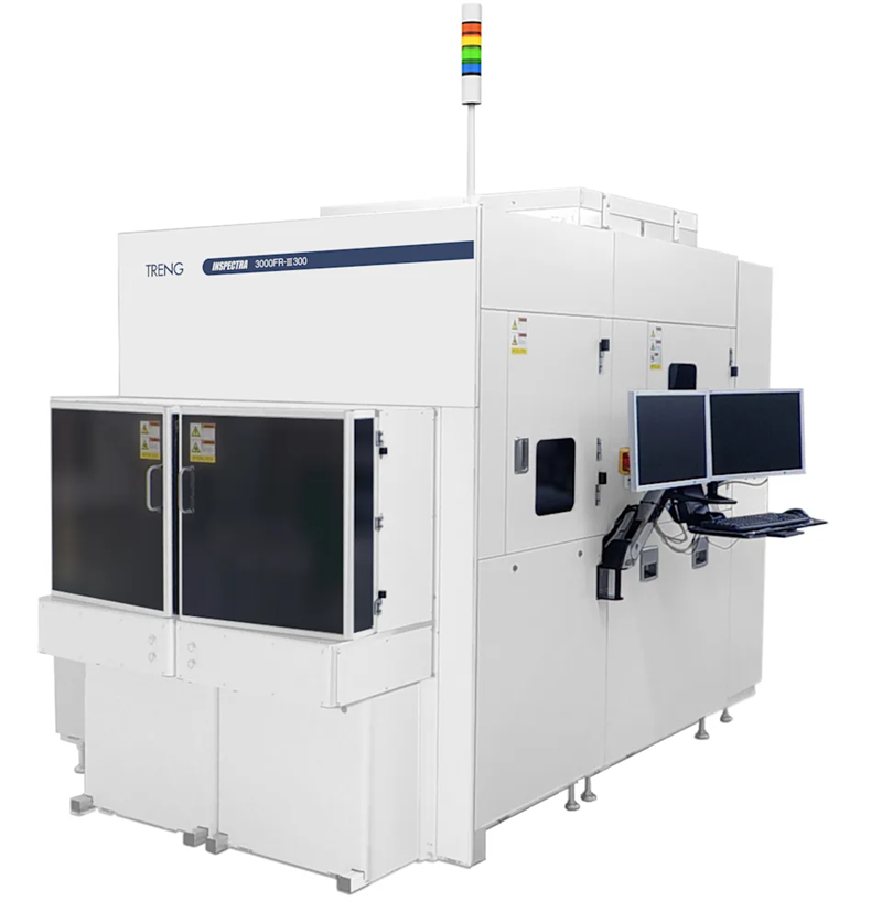
However, glass substrates are susceptible to microscopic cracks, which can compromise semiconductor stability and necessitate removal during processing. Traditional optical inspection methods could only detect surface defects. TASMIT's new system, building on the INSPECTRA® series, incorporates a novel defect detection and analysis algorithm and a polarized light-based optical inspection mechanism, enabling the first-ever double-sided and internal defect inspection. It maintains the series' high inspection speed of 40 seconds per panel, ensuring 100% inspection and preventing defective products from reaching the market. For PCB manufacturers, this means higher reliability and reduced waste in high-density packaging processes.
")
About TASMIT, Inc.:
Established in July 2000 as a subsidiary of Toray Engineering, TASMIT, Inc. specializes in semiconductor inspection equipment. The company offers high-quality solutions for semiconductor device manufacturing through its core products: the "INSPECTRA" optical semiconductor wafer inspection system and the "NGR" electron beam semiconductor wafer pattern verification system, both leveraging robust semiconductor inspection technologies. With this latest innovation, TASMIT is poised to become a key partner for PCB manufacturers navigating the challenges of next-generation high-density packaging.
+86 191 9627 2716
+86 181 7379 0595
8:30 a.m. to 5:30 p.m., Monday to Friday

