-advertisement-
Absolics, an affiliate of SKC, the leading South Korean chemical and materials company, has been granted an unprecedented $75 million subsidy under the U.S. CHIPS Act. Remarkably, Absolics, a company specializing in materials, components, and equipment (SoC), has become the first non-semiconductor chip manufacturer to receive this subsidy.
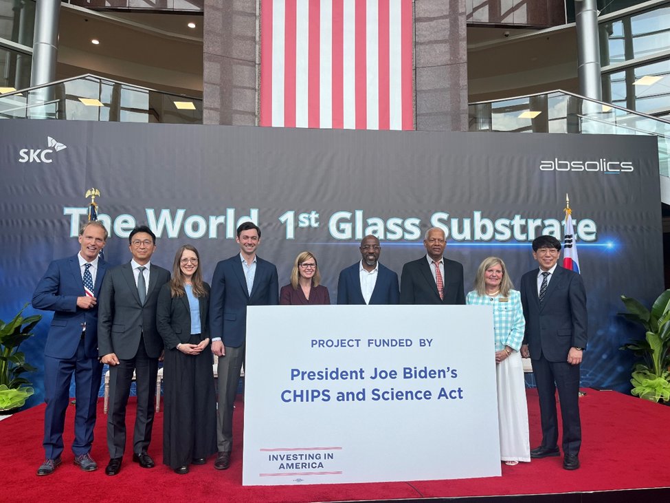
The U.S. Department of Commerce revealed on May 23rd the subsidy plan for Absolics' state-of-the-art semiconductor packaging glass substrate production plant in Covington, Georgia.
The funding is part of a larger $52.7 billion U.S. government initiative aimed at spurring U.S. semiconductor chip manufacturing. Besides fortifying the semiconductor supply chain with new advanced materials, the funds will generate significant employment opportunities in Covington, Georgia, with an estimated 1,000 construction jobs and 200 manufacturing and R&D roles in the offing.
Absolics’ Covington Plant 1, which received the subsidy, is the world’s first mass production facility for glass substrates, with an annual production capacity of 12,000 square meters. Absolics, which broke ground on the Covington plant in November 2022, has recently completed Plant 1 and is currently in trial operation. The company plans to complete its own sample testing in the second quarter and begin full-scale customer certification in the second half of this year.
CEO Jun Rok Oh revealed in a statement that the proposed funding will enable the company to commercialize their pioneering glass substrate technology fully. This tech allows processing and memory chips to be packaged as a single device, which improves computing speed and efficiency. The Commerce Department iterated that Absolics' glass substrates will be utilized to enhance the performance of leading-edge chips for AI and data centers.
In a move to regain control in a market currently concentrated in Asia, the advanced packaging substrates, as highlighted by U.S. Commerce Secretary Gina Raimondo, are set to become a priority. She declared last year that "the U.S. will develop multiple high-volume advanced packaging facilities." This came on the heels of the announcement from the world's second-largest memory chip maker, SK Hynix (000660.KS), that it intends to invest $3.87 billion in constructing an advanced packaging plant and R&D facility for AI products in Indiana.
Editor:Lulu
▼▼▼
China's largest chipmaker SMIC is now the No. 3 foundry in the world, Counterpoint says
Nvidia cuts China AI chip prices amid competition from Huawei
South Korea announces $19 billion support package for chip industry
Tesla's oldest factory ignites another headline by catching fire
Samsung Electronics names new chief for semiconductor business as AI chip race heats up
Tokyo Electron plans to set aside $1.6 billion for R&D this year
+86 191 9627 2716
+86 181 7379 0595
8:30 a.m. to 5:30 p.m., Monday to Friday

