At the Mobile World Congress (MWC) 2025 in Barcelona, Spain, SKC and CIT, two leading South Korean advanced materials companies, are drawing global attention with their groundbreaking glass substrate technologies, positioning themselves as key players in the future of AI and semiconductor industries.
SKC’s Glass Substrate: A Game-Changer for AI Data Centers
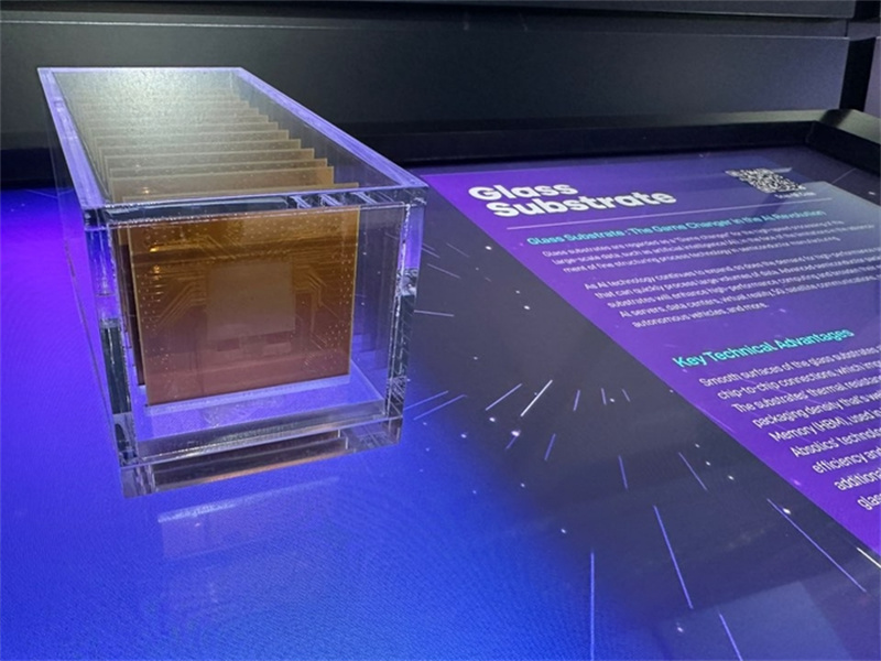
SKC, a pioneer in semiconductor glass substrates, is showcasing its innovative glass substrate technology at the MWC 2025 exhibition. The company is highlighting its glass substrate as a core solution for AI data centers, emphasizing its ability to handle massive data processing demands. The substrate, displayed alongside SK Hynix’s high-bandwidth memory (HBM3E) and high-performance SSDs, forms part of an integrated AI solution.
The glass substrate enables ultra-fine circuit implementation and integrates components such as multi-layer ceramic capacitors (MLCCs), allowing for the mounting of high-capacity CPUs and GPUs. Compared to traditional substrates, SKC’s glass substrate reduces power consumption and package thickness by more than half while improving data processing speeds by 40%.
An SKC representative stated, “As the world’s first company to commercialize semiconductor glass substrates, we aim to demonstrate our technological excellence at MWC 2025, following our success at CES 2025. We expect our commercialization efforts, targeted for the end of this year, to significantly contribute to the advancement of AI technologies globally.”
CIT’s Advanced Glass Substrate and Copper Deposition Technology
Meanwhile, CIT, a South Korean advanced materials startup, is also making waves at MWC 2025 with its proprietary Atomic Sputtering Epitaxy (ASE) technology. CIT’s glass substrate, featuring a 0.62mm thickness, 100μm hole size, and 6:1 aspect ratio, is precision-engineered for high-performance applications. The company has achieved uniform copper deposition with a thickness of 1,000nm and a surface resistance of 0.01Ω/sq, ensuring stable electrical performance.
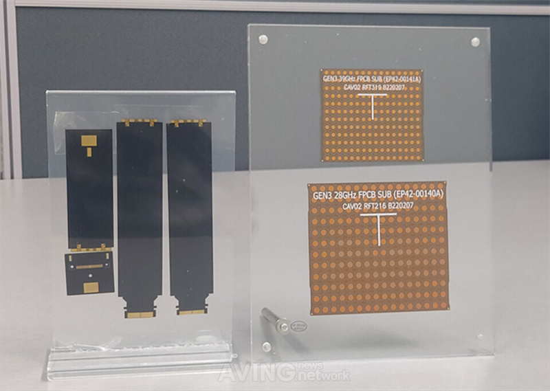
CIT is unveiling three key products at MWC 2025:
Transparent Antenna (Dolphin): Awarded the CES 2025 Innovation Award, this antenna is 1,000 times thinner than conventional vehicle antennas while offering 20% improved signal reception. Enhanced with the “Etalon” structure, it boasts increased heat and weather resistance, making it suitable for curved and stretchable environments.
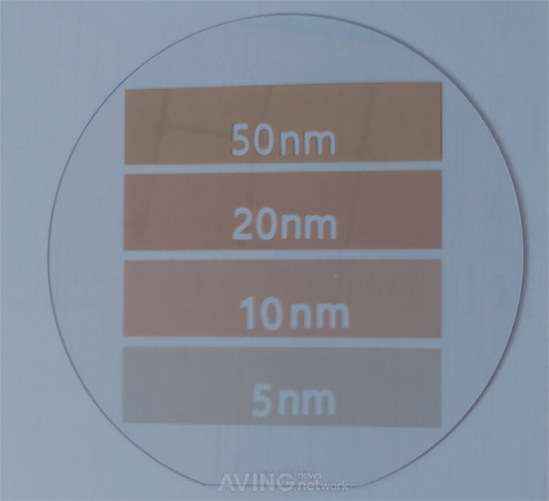
1. Ultra-Thin Copper Film: With a thickness as low as 5nm (1/2000th of a human hair), this film delivers exceptional conductivity and is ideal for next-generation semiconductor applications.
2. Transparent Display: Featuring ultra-thin copper circuits, this display is nearly invisible to the human eye and targets applications in exhibitions, industrial facilities, and public transportation.
3. CIT’s glass substrate technology also supports through-glass via (TGV) copper deposition with a 6:1 aspect ratio, eliminating the need for a seed layer and significantly improving process efficiency.
A Shared Vision for the Future
Both SKC and CIT are driving innovation in the semiconductor and AI industries with their glass substrate technologies. As the demand for faster signal transmission and improved power efficiency grows, glass substrates are emerging as a next-generation solution for advanced packaging and high-performance computing.
With SKC targeting commercialization by the end of 2025 and CIT gaining international recognition through awards and publications in Nature Communications, South Korea is solidifying its position as a global leader in advanced materials and semiconductor technologies.
The MWC 2025 exhibition not only highlights the technological prowess of these companies but also underscores the critical role of glass substrates in shaping the future of AI, data centers, and next-generation electronics. As the AI semiconductor era unfolds, SKC and CIT are poised to play pivotal roles in driving innovation and meeting the growing demands of the global tech industry.
+86 191 9627 2716
+86 181 7379 0595
8:30 a.m. to 5:30 p.m., Monday to Friday

