
-advertisement-

SK hynix Inc.(000660.KS)is set to convert one of its main DRAM production lines at its Icheon facility in South Korea to produce high-bandwidth memory (HBM), due to growing demand.
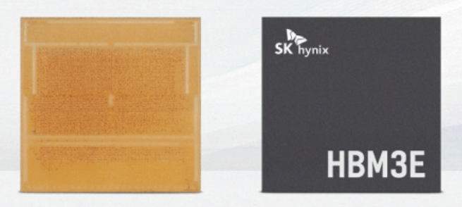
The M10F line, currently undergoing modifications to produce HBM3E, is expected to have the necessary equipment installed by the first quarter of next year, with production slated to begin in the fourth quarter of 2025, sources said.
SK Hynix supplies HBM, used in AI inference applications, to major clients including Nvidia, Google, and Amazon. The company has previously reported receiving requests from these tech giants for customized HBM solutions.
The M10F line will likely have a capacity of 10,000 wafers per month for HBM production. Once fully operational, SK Hynix’s overall HBM production capacity will reach 150,000 wafers per month.
However, further expansion of HBM capacity beyond the M10F line is not expected. Competitors Samsung and Micron are also ramping up HBM production, and China’s CXMT has announced plans to enter the market as well, suggesting that current capacity is sufficient to meet demand.
SK Hynix plans to focus on producing the most advanced HBMs, phasing out older products to maintain its competitive edge, company insiders said.
Editor:Lulu
▼▼▼
Exclusive: Qualcomm has explored buying pieces of Intel chip design business
TSMC and Samsung partner to develop next-generation HBM4 for AI chip advancements
VIS and NXP announce establishment of VSMC joint venture
Q2 2024 global semiconductor billings increased: SEMI report
PSMC's Logic-DRAM technology adopted by AMD and global leaders to power next-gen AI chips
Samsung said to slash 8% of sales team in mainland China amid weak performance
+86 191 9627 2716
+86 181 7379 0595
8:30 a.m. to 5:30 p.m., Monday to Friday

