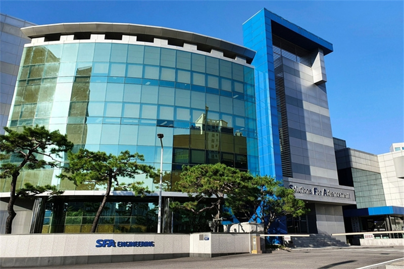
South Korean company SFA, a leader in smart factory and automation solutions, has entered the advanced semiconductor packaging metrology and inspection (MI) equipment market. The company recently developed three types of inspection equipment specifically designed for high-bandwidth memory (HBM) and glass substrate production processes. One of these systems was supplied to a major domestic semiconductor company.
In an interview on March 31, Choi Ho-chul, Head of SFA's R&D Center 1, explained, “We recently supplied a White Light Interferometry (WLI)-based bump height measurement system to a large domestic company, and we plan to deliver four more units.” He added, “This equipment can measure minute height differences in bumps and step heights at a nanometer scale, which is crucial for the HBM and glass substrate packaging processes.”
WLI technology uses interference patterns created when light reflected from different paths overlaps. This allows for precise surface height measurement with high axial resolution. The use of white light, which includes various wavelengths, provides even finer resolution compared to single-wavelength systems. The light splits into two paths—one reflected from a reference mirror and the other from the surface being inspected. The interference patterns are captured by a camera, and software converts this data into 3D step information.
HBM, which stacks multiple DRAM dies vertically, requires precise bump height measurement to ensure good yield, as defects in interlayer bonds can render the entire product defective. The WLI equipment measures bump height uniformity quickly and accurately before chips are stacked, preventing defects from arising.
The system is also useful in glass substrate processing, which is prone to warping due to its large surface area. WLI can scan the entire surface at high speed, precisely measuring distortion and step height uniformity. The system is also capable of inspecting very thin and intricate structures, such as those in the Through-Glass Via (TGV) process, without damage. Furthermore, it accurately measures groove depth, width, and step height in the substrate, making it ideal for precision verification of structures formed through laser processing or etching.

SFA's WLI system stands out due to its inline inspection capability. Unlike offline systems that require separate analysis steps and can cause production delays, inline inspection integrates directly into the production line, allowing for real-time measurements, automatic decision-making, and automatic transfer—all without halting the manufacturing process.
“Most step height measurement systems operate as independent analyzers, limiting productivity,” said Choi. “SFA leveraged its expertise in large-scale substrate handling from the display and secondary battery sectors, as well as high-speed optical design, to optimize WLI equipment for inline environments.”
Although the specific processes for which the equipment will be used at the domestic semiconductor company have not been disclosed, its potential applications across both semiconductor packaging and glass substrate processes are vast.
In addition to WLI equipment, SFA has also developed X-ray 3D CT inspection equipment and SEM-based tools, completing its portfolio in the semiconductor packaging MI field. All these tools operate in an inline configuration, allowing for real-time inspection within the production process without the need for separate analysis.
The 3D CT equipment enables non-destructive internal defect inspection, critical for processes like TGV in glass substrates and TSV in HBM production. It can detect the status of internal conductive materials or voids in real-time. With inspection times reduced to under four minutes per point—compared to several hours for traditional methods—this equipment is expected to attract interest from companies in the HBM and glass substrate sectors. SEM equipment, combined with AI, can automatically identify potential defects, provide high-magnification imaging, and perform elemental analysis.
Choi concluded, “We expect to generate over 10 billion KRW in sales from the semiconductor packaging MI sector this year. Our goal is to secure new annual revenue streams of 200 to 300 billion KRW (approximately 1 to 1.49 billion CNY or 136 to 203 million USD) in this field within the next five years.”
+86 191 9627 2716
+86 181 7379 0595
8:30 a.m. to 5:30 p.m., Monday to Friday
