-advertisement-
June 24, 2024: To achieve a CO2-neutral world and an All-Electric Society, innovations like high power densities, reduced losses, and cost advantages are essential. Collaboration among companies in these technology areas is crucial for a sustainable energy transition. Two traditional microelectronics companies are now forming a strategic partnership in power embedding, aiming to enhance efficiency with the p² Pack® embedding technology.
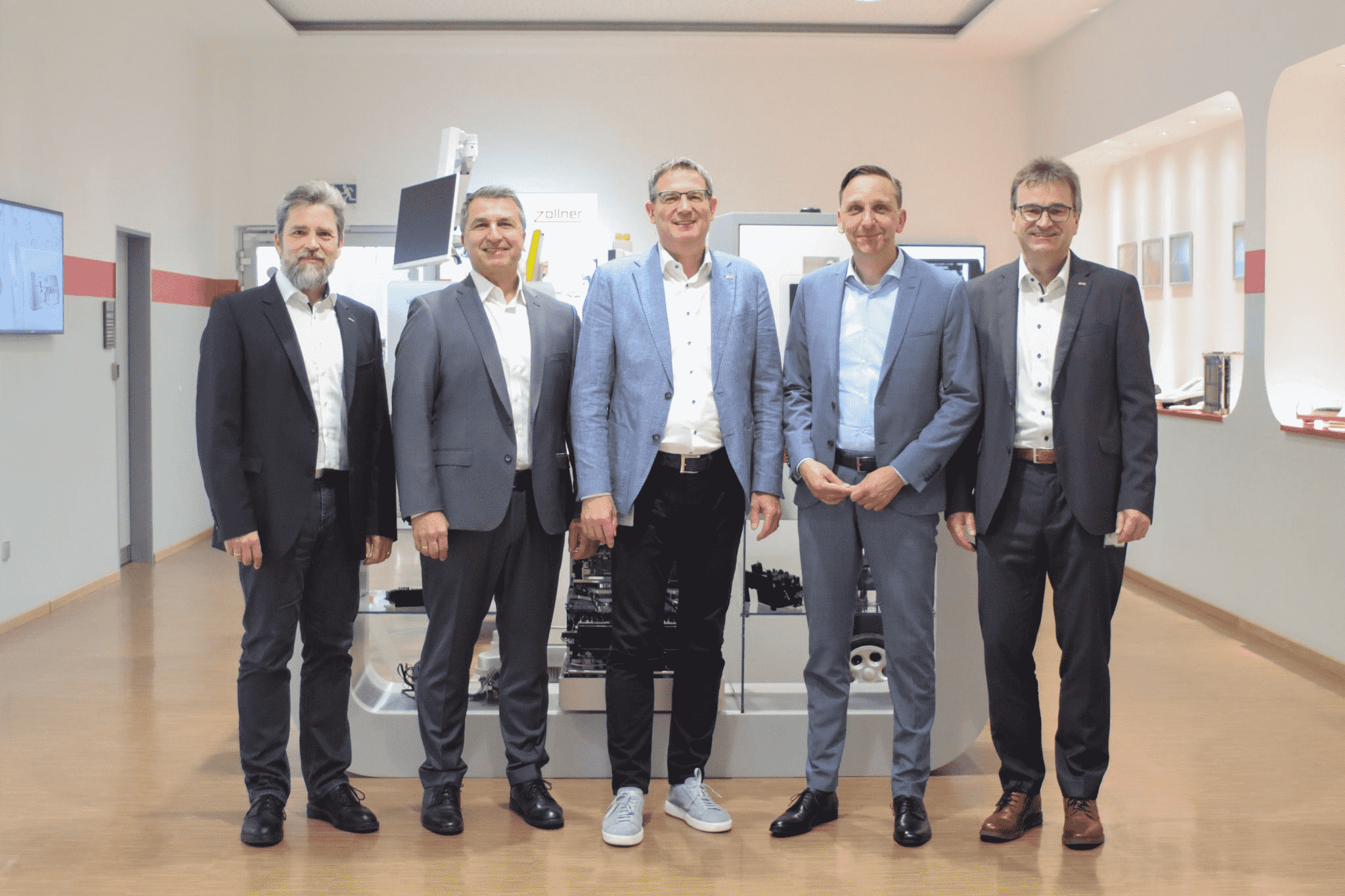
This partnership between Schweizer Electronic AG (SCE) and Zollner Elektronik AG will leverage Schweizer's p² Pack® technology, integrating SiC chips into printed circuit boards for high power switching applications, especially in DC-AC conversions. This technology promises high energy efficiency, reliability, and long service life, already proven by major Tier-1 companies in Europe.
The collaboration will allow Zollner to integrate this technology into their applications and support customers transitioning from traditional to embedding designs, maximizing benefits. This partnership is a significant growth opportunity, fostering new applications and expanding the customer base.
Nicolas-Fabian Schweizer, CEO of Schweizer Electronic AG, and Ludwig Zollner, CEO of Zollner Elektronik AG, both express optimism about the partnership, emphasizing the synergy and innovation potential it brings, benefiting both companies and their customers.

About SCHWEIZER
The company was founded by Christoph Schweizer in 1849 and is listed at the Stuttgart and Frankfurt Stock Exchanges (ticker symbol “SCE”, “ISIN DE 000515623”).
Schweizer Electronic AG offers the latest, cutting-edge technology and consultancy expertise in the PCB industry. Thanks to its state-of-the-art production facilities in Schramberg, Germany and Jintan, China as well as close partnerships with other technology leaders.
The SCHWEIZER (smart) p² Pack is a technology for the embedding of power semiconductors into PCBs. This procedure is not simply a new packaging method. More importantly, it allows power electronics systems to be developed in accordance with a completely different philosophy. Applications developed with the smart p² Pack technology enable higher power levels, compact designs, and a high integration depth. The production chain for system suppliers and the lay-up and interconnection technology in the system are greatly simplified as a result. In addition, there are potential cost savings at system level.
Editor:Lulu
▼▼▼
Welgao Thailand factory grandly opens today!
North American PCB industry sales down 6.8 percent in May
University of Tokyo and partners develop new technique for drilling package substrates
Customs commissioner visits Simmtech to address import and export challenges
India's push to limit Chinese PCB imports faces resistance from automakers
Driven by the expansion of rigid PCB sales, BH will achieve strong medium to long-term growth
+86 191 9627 2716
+86 181 7379 0595
8:30 a.m. to 5:30 p.m., Monday to Friday

