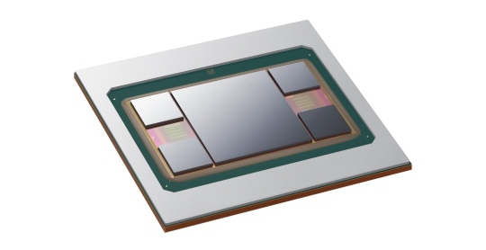
Samsung has won Nvidia as a customer for 2.5D packaging.
The company’s Advanced Package (AVP) team will be providing the interpose and I-Cube, its 2.5D package to the GPU maker, sources said.
The high bandwidth memory (HBM) and the GPU wafer production will be handled by other companies.
A 2.5D package has the chip dies CPU, GPU, I/O, HBM, and others placed horizontally on an interposer.
TSMC calls its 2.5D package technology chip-on-wafer-on-substrate (CoWoS), while Samsung calls theirs I-Cube.
Nvidia’s A100 and H100 are made with this packaging technology and so is Intel Gaudi.
Samsung worked since last year to secure customers for its 2.5D packaging service.
The tech giant proposed to customers that it would allocate sufficient staff to the AVP team while offering its own interposer wafer design.
Samsung will provide a 2.5D package with four HBM chips placed on them for Nvidia, sources said.
The South Korean tech giant already has the packaging technology to place eight HBM chips, they added.
Meanwhile, to mount eight HBM chips on a 12-inch wafer, there need to be 16 interposers, which can downgrade production efficiency, they also said.
So Samsung was developing a panel-level package technology for the interposer when the number of HBM chips reached eight.
Nvidia likely gave the order to the South Korean tech giant due to the demand increase for its AI chips, which means TSMC’s CoWoS capacity will be insufficient.
The order could also open up Samsung to win orders for HBMs.
Editor:Vicky
▼▼▼
ASML set to comply with U.S. demands on China exports
Samsung wins Nvidia’s 2.5D package order
Intel confirms new round of layoffs in its Sales and Marketing Group
WT Microelectronics completes acquisition of Future Electronics
Nvidia supplier SK Hynix to invest $3.87 bln in US chip packaging plant
TSMC's evacuated workers return to some factories after Taiwan's strongest earthquake in 25 years
+86 191 9627 2716
+86 181 7379 0595
8:30 a.m. to 5:30 p.m., Monday to Friday
