Samsung Electronics Co., the world’s largest memory chipmaker, has won its first 2-nanometer node artificial intelligence chip production contract from Japanese startup Preferred Networks Inc. (PFN) – a big win over Taiwan Semiconductor Manufacturing Co. (TSMC) in the race for advanced chip processing technology.
Under the deal, Suwon, South Korea-based Samsung will make AI accelerators and other AI chips with its latest 2 nm chip processing tech for PFN, industry sources said on Friday.
PFN has been collaborating with TSMC since 2016 but it decided to produce its next-generation AI chips on Samsung’s 2 nm node, a person familiar with the matter said.
The deal benefits both as PFN could gain access to newer chip technologies that will allow it to gain the edge against the competition, while Samsung has secured an actual customer for its most advanced chip tech, gaining ground in foundry against TSMC, sources said.
Established in 2014, PFN is known for its expertise in AI deep learning development and has attracted large-scale investments from major companies, including Toyota Motor, NTT and FANUC, a Japanese robot system maker.
Sources said PFN decided to forgo TSNC as Samsung provides a comprehensive chip-making service on a turnkey basis, from chip design to production and advanced chip packaging.
Samsung officials declined to confirm its deal with PFN.
DEAL OPENS DOOR FOR MORE 2 NM CLIENTS
Analysts said while TSMC currently has more 2 nm clients, PFN's switch to Samsun could signal a reversal in Samsung’s favor, opening the door for more important clients to side with the Korean chipmaker.

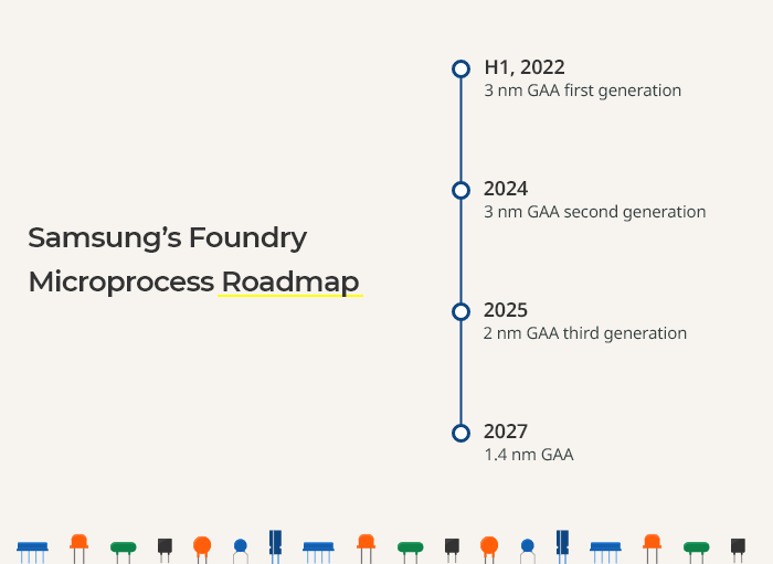
Samsung's foundry microprocess roadmap
TSMC is the leader in the contract chipmaking arena grabbing the most business from fabless chip designers such as Apple Inc. and Qualcomm Inc.
With the demand for high-performance chips rising, competition for technology advancement is fierce, particularly between TSMC and Samsung.
The Taiwanese chipmaker is ahead of Samsung by providing chips made with its 2 nm tech to its clients such as Apple and Nvidia. TSMC aims to begin mass production of chips with 2 nm tech in 2025.
Samsung also said it will begin mass production of the 2 nm process for mobile applications in 2025 before expanding to other uses in later years.

Samsung's foundry business chief Choi Si-young unveils a new tech roadmap at Samsung Foundry Forum 2022
Samsung said it will apply the advanced 2 nm technology to high-performance computing (HPC) chips for supercomputers and computer clusters in 2026 and then to automotive chips in 2027.
Samsung plans to begin mass production of more advanced 1.4 nm chips by 2027.
Chipmaking processes carry a numerical label that loosely denotes the size of the transistors that can be packed on a chip. The number refers to the thickness of the circuitry that can be drawn on the transistor. The lower the number, the more advanced the technology.
While Samsung’s production tech is based on GAA transistor architecture for its microfabrication process, TSMC uses a different technology in the fin field-effect transistor (FinFET) structure.
“From the 2-nanometer node, the foundry leader will also adopt the GAA technology. We will overtake TSMC with our tech within the next five years,” Kyung Kye-hyun, chief of Samsung’s Device Solutions division that oversees semiconductors, said at a speech in Korea last year.
▼▼▼
German Court bans sales of select Intel CPUs in Germany over patent dispute
TSMC to build second Japan chip factory, raising investment to $20 billion
Heart-on-a-chip: A microfluidic marvel shaping the future of cardiovascular research
+86 191 9627 2716
+86 181 7379 0595
8:30 a.m. to 5:30 p.m., Monday to Friday
