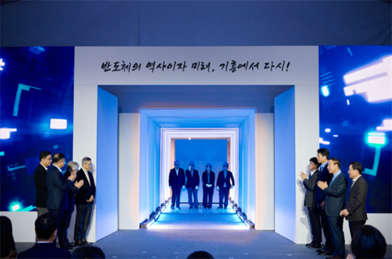
Samsung Electronics Co., the world's largest memory chipmaker, recently held a "tool-in" ceremony for its new semiconductor research and development (R&D) complex, NRD-K, located at the Giheung campus near Seoul. This event celebrated the installation of the first batch of equipment, marking the transition from construction to manufacturing readiness for the cutting-edge facility.
Construction of the NRD-K complex began in 2022, covering 109,000 square meters within Samsung's Giheung campus. The facility is set to be a key R&D hub for Samsung's memory, system large-scale integration (LSI), and foundry semiconductor divisions. With a planned investment of 20 trillion won (approximately $14.4 billion) by 2030, the complex is expected to be fully operational by mid-2025. It will feature advanced technology, including high Numerical Aperture (NA) extreme ultraviolet (EUV) lithography machines and sophisticated wafer bonding infrastructure, supporting the development of next-generation semiconductors such as 3D DRAM and V-NAND with more than 1,000 layers.
At the ceremony, Samsung Vice Chairman Young Hyun Jun emphasized the company's ambition to accelerate research on future technologies and streamline the transition from research to mass production. He noted that NRD-K will enhance development speed, supporting Samsung's strategy of rapid innovation in the semiconductor field. The Giheung campus, which produced the world's first 64Mb DRAM in 1992, has been central to Samsung's leadership in the semiconductor industry, and the new facility aims to continue that legacy.

Samsung's investment in the NRD-K complex reflects its broader commitment to technological leadership. In the third quarter of this year, the company invested a record 8.87 trillion won in R&D, focusing on cutting-edge technologies like advanced packaging for high bandwidth memory (HBM) production.

The tool-in ceremony also highlighted Samsung's focus on strategic partnerships within the semiconductor ecosystem. The event included around 100 guests, featuring representatives from suppliers and customers. Park Gwang-Sun, head of Applied Materials Korea, a major Samsung partner, emphasized the importance of collaboration, stating that deep cooperation with Samsung will drive future growth in the semiconductor industry.
With NRD-K, Samsung aims to consolidate advanced research, product development, and manufacturing in one facility, driving faster innovation cycles and reinforcing its position as a leading force in the semiconductor sector. The establishment of this complex is expected to set the stage for continued leadership in technology over the next century.
+86 191 9627 2716
+86 181 7379 0595
8:30 a.m. to 5:30 p.m., Monday to Friday
