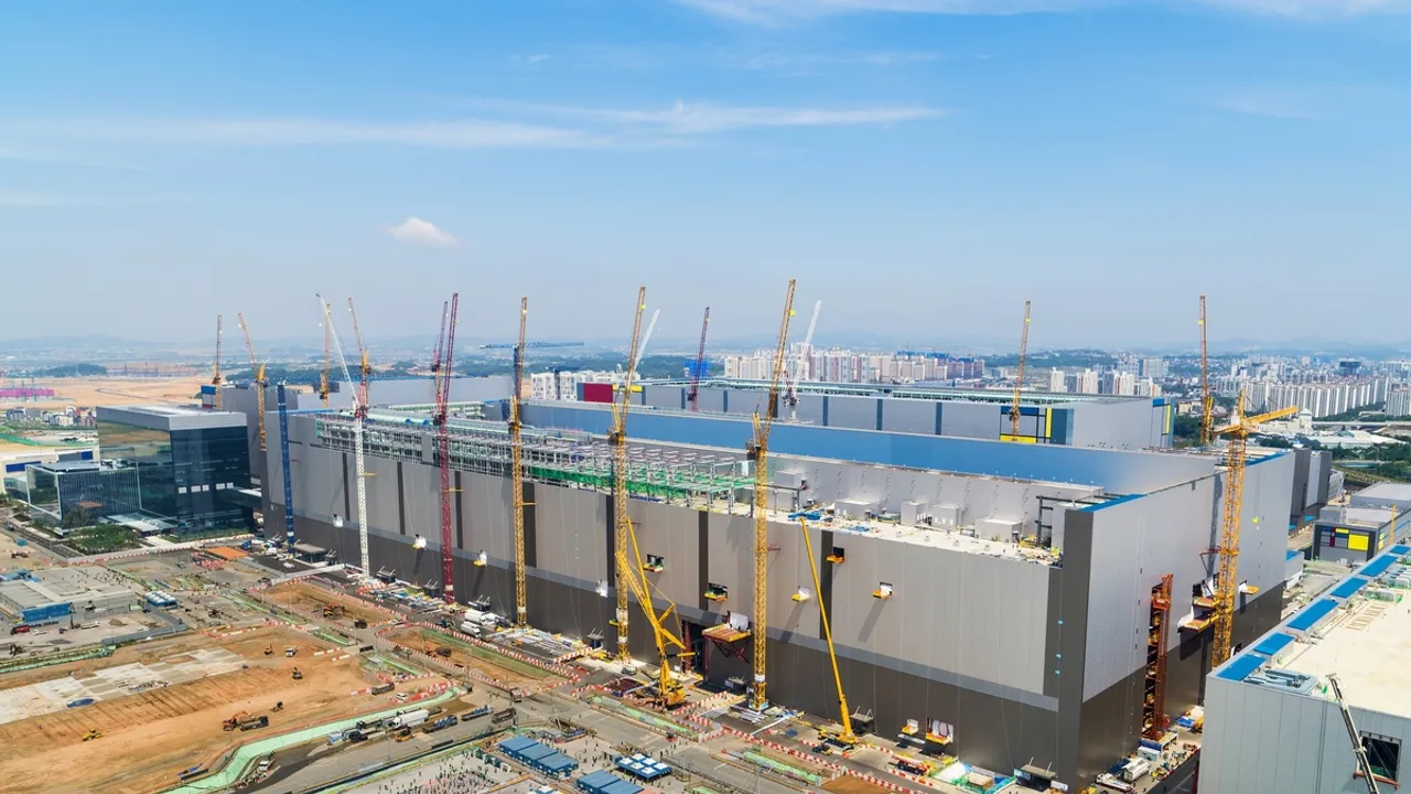
Samsung Electronics Revises Construction Plans Amid Semiconductor Market Fluctuations in Pyeongtaek, South Korea
In an unexpected pivot reflecting the current semiconductor market dynamics, Samsung Electronics has announced a significant revision to its construction schedule at the Pyeongtaek Plant 4 (P4) in South Korea. This strategic adjustment comes as the technology giant grapples with the ebb and flow of global demand, underscoring the challenges and uncertainties within the semiconductor industry.
Strategic Shift in Construction Priorities
The original plan for the Pyeongtaek Plant 4 (P4) included the construction of the PH2 cleanroom, which was targeted for semiconductor contract manufacturing. However, in a decisive response to market conditions detailed in its fourth-quarter financial report for 2023, Samsung has opted to delay the PH2 project. Instead, the focus will now shift towards the development of the PH3 cleanroom, earmarked for DRAM and other memory production lines. This alteration in the construction sequence not only highlights Samsung's agility in navigating market fluctuations but also underscores the importance of DRAM and memory products in its portfolio.
Challenges Beyond the South Korean Border
Further complicating Samsung's operational landscape is the delay in the commencement of mass production at its eagerly anticipated semiconductor fabrication facility in Taylor, Texas. Initially slated to begin in the second half of 2024, the timeline has now been pushed to 2025. The reasons for this delay remain unspecified, but reports suggest difficulties in securing subsidies from the US government as a potential factor. This setback in the United States mirrors the broader challenges Samsung faces, as it recalibrates its strategies in light of global semiconductor market conditions.
Market Realities and Financial Implications
The semiconductor market's recovery pace varies significantly across different industries, compelling major players like Samsung Electronics to adapt swiftly. The company's latest financial report paints a mixed picture. While the memory business has seen improvements thanks to high-added-value products such as HBM, the foundry segment continues to struggle. The Device Solutions unit reported a substantial loss of KRW2.18 trillion (US$1.64 billion), indicating the scale of challenges Samsung confronts. The construction schedule adjustments at P4 and the temporary suspension of P5 construction are strategic moves to mitigate these losses and align with the current market trajectory.
In the face of these tumultuous times, Samsung Electronics' decision to recalibrate its construction and production plans is a testament to its resilience and adaptability. As the company navigates through the semiconductor market's uncertainties, its strategic adjustments in South Korea and abroad will be closely watched by industry observers and stakeholders alike. The technology titan's journey through these challenges may well set the pace for the global semiconductor industry's path forward.
▼▼▼
Samsung wins first 2 nm AI chip order from Japan’s PFN; a slap on TSMC
German Court bans sales of select Intel CPUs in Germany over patent dispute
TSMC to build second Japan chip factory, raising investment to $20 billion
Heart-on-a-chip: A microfluidic marvel shaping the future of cardiovascular research
+86 191 9627 2716
+86 181 7379 0595
8:30 a.m. to 5:30 p.m., Monday to Friday
