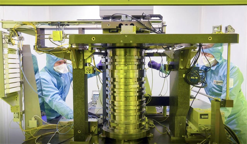
Russia has successfully completed the development of its first 350nm lithography machine, a crucial step toward semiconductor self-sufficiency. Moscow Mayor Sergei Sobyanin announced the breakthrough on March 24 (local time in Russia) via his Telegram channel, crediting Zelenograd Nanotechnology Center for leading the project.
A Response to Western Sanctions
Following the Russia-Ukraine conflict, the U.S. and Western nations imposed strict export controls on advanced technology, particularly targeting semiconductors and lithography machines. This prompted Russia to accelerate efforts to build its own domestic alternatives.
In 2023, Vasily Shpak, Deputy Minister of Industry and Trade, revealed that Russia planned to start producing 350nm lithography machines in 2024, followed by 130nm models in 2026. Production is set to take place across Moscow, Zelenograd, Saint Petersburg, and Novosibirsk.
By May 2024, Shpak announced at the CIPR 2024 conference that the first machine had been assembled and was undergoing testing. Details were scarce at the time, but Sobyanin's latest statement confirms that the development is now complete — with photos of the machine released to the public.
A Technological Breakthrough
Sobyanin highlighted that fewer than 10 countries can manufacture such vital chip production equipment, and Russia has now joined this elite group.
"We've taken a major step toward self-sufficient microelectronics production and full technological sovereignty," Sobyanin said.
He also pointed out a key innovation: unlike traditional foreign models that use mercury lamps as light sources, Russia's machine employs a solid-state laser — offering higher power, better energy efficiency, greater durability, and a narrower light spectrum for enhanced precision.
The machine features an expanded 22mm × 22mm working area and supports wafers up to 200mm in diameter — essential for producing chips used in automotive, energy, and telecommunications sectors, where mature nodes like 350nm remain widely used.

Production and Future Plans
Anatoly Kovalev, General Director of Zelenograd Nanotechnology Center, confirmed the project was completed under a state contract in collaboration with Belarus-based Planar. The machine successfully passed testing in December 2024, meeting all declared technical specifications.
Kovalev added that the machine is already being tailored to meet specific customer requirements, with production now gearing up for larger-scale manufacturing. Additionally, the center is working on a 130nm lithography machine under a second government contract, aiming for completion in 2026.
Russia has allocated 2.114 trillion rubles (approximately $23 billion) in 2024 to fund domestic electronics development — including expanding 350nm production and advancing toward 130nm capabilities.
Why Focus on 350nm to 65nm Lithography?
Russia's strategy prioritizes lithography machines between 350nm and 65nm, targeting chips essential for microcontrollers, power electronics, telecommunication circuits, and automotive systems — sectors accounting for 60% of global semiconductor demand. These nodes are expected to stay relevant for at least the next decade.
Shpak emphasized:
"Without semiconductor sovereignty, there's no technological sovereignty — and without that, national defense and political sovereignty become fragile."
He acknowledged that while Russia already possesses the know-how to produce 65nm chips using foreign equipment, export bans on advanced machines mean domestic production capabilities are now a necessity.
Moscow's Role in Russia's Microelectronics Future
Anatoly Gorbuzov, Moscow's Minister of Investment and Industrial Policy, praised the development, calling Moscow “the center of Russia's microelectronics industry”, contributing 40% of the country's total revenue in the sector.
Gorbuzov emphasized that advancements in microelectronics and photonics are set to drive innovation across industries — from optical communications and sensor technology to radio photonics. He highlighted Moscow Technopolis as a growing economic hub, where companies are "implementing strategic projects focused on producing technologies essential to Russia's future."
With its first domestic lithography machine completed and larger-scale production on the horizon, Russia has taken a significant step toward reshaping its semiconductor industry — aiming for long-term technological independence.
+86 191 9627 2716
+86 181 7379 0595
8:30 a.m. to 5:30 p.m., Monday to Friday
