A South Korean manufacturer of high-tech equipment, Philoptics (KOSDAQ: 161580) has announced the appointment of Lim Baek-gyun, former Vice President and Head of Samsung SDI's Manufacturing Innovation Center, as the new head of its semiconductor equipment division. Starting next month, Lim will join the company as President, overseeing Philoptics' efforts to expand its market presence in semiconductor equipment, including its core DI lithography equipment and glass substrate Through Glass Via (TGV) solutions.
Born in 1963, Lim brings extensive experience from his tenure at Samsung Electronics and Samsung SDI. He previously served as Head of Memory Manufacturing Center at Samsung Electronics' DS Division and later collaborated with Jeon Young-hyun, now Vice Chairman of Samsung Electronics, at Samsung SDI, where Lim led large-scale battery manufacturing innovation.
This leadership transition follows the promotion of Philoptics’ founder, Han Ki-soo, to Chairman. Meanwhile, its subsidiary, Phil Energy, also announced key promotions: CEO Kim Kwang-il became Vice Chairman, while Vice President Kim Do-young was promoted to President. With its battery equipment business running steadily, Philoptics is now focusing on semiconductor equipment to drive new growth, as the company faces challenges in expanding its traditional display equipment segment.
Focus on TGV Technology for Glass Substrates
Philoptics is positioning itself as a leader in TGV laser drilling equipment, which is used to create microscopic holes in glass substrates for electrode pathways. The company has already secured a significant client, Appsolix, a joint venture between SKC and Applied Materials, to advance its glass substrate solutions.
Glass substrates are gaining traction as an alternative to traditional organic or silicon-based materials due to their superior thermal and mechanical stability. They are particularly well-suited for high-performance semiconductors, thanks to their ability to support fine circuits and larger designs. However, processing glass substrates is technically demanding, as it involves precision drilling without causing cracks and seamless copper plating for electrode formation.
Major semiconductor players, including Samsung Electronics, SK hynix, and Intel, are expected to adopt glass substrates starting in 2026. This has intensified competition in the glass substrate equipment market. Philoptics is proactively seeking new clients and aims to refine its technology to maintain consistent quality while reducing processing times for various hole sizes and shapes.

Financial Challenges and Strategic Shifts
Philoptics reported an estimated revenue of ₩54 billion (approximately $42 million) in 2023, down from ₩115.2 billion in 2022 and ₩104 billion in 2021. This decline underscores the need for diversification beyond its battery equipment business. Industry experts emphasize that Philoptics must actively explore and develop new business opportunities to regain growth momentum.
With Lim’s extensive expertise and the company’s focus on TGV technology, Philoptics is positioning itself to capture emerging opportunities in the evolving semiconductor market. However, its success will depend on securing more clients and overcoming technical challenges in glass substrate processing.
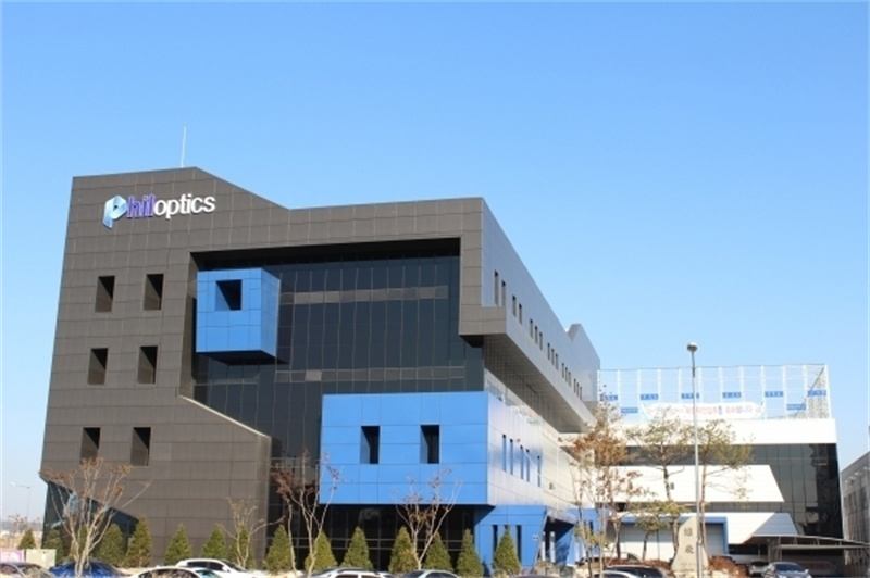
Philoptics Co., Ltd. (161580.KQ), established in 2009 and headquartered in Gyeonggi-do, South Korea, is a manufacturer of high-tech equipment primarily serving the display, printed circuit board (PCB), semiconductor, and battery industries. The company operates two main sales divisions: the Display Department, which oversees the technical sales and management of display processing equipment both domestically and internationally, and the Technical Department, which handles the technical sales and management of PCB and touch screen panel (TSP) processing equipment. Recently, Philoptics has expanded into semiconductor equipment and battery equipment, positioning itself as a key player in emerging markets like glass substrates and advanced laser processing technologies.
+86 191 9627 2716
+86 181 7379 0595
8:30 a.m. to 5:30 p.m., Monday to Friday

