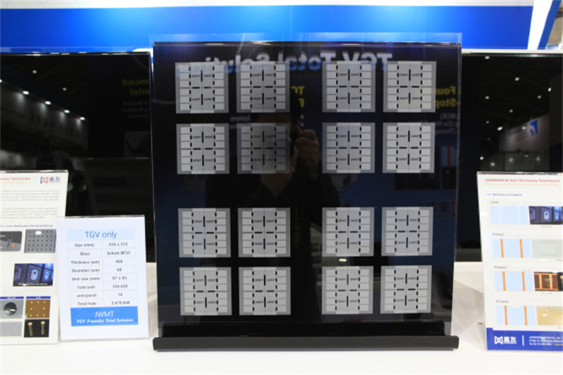
Sourh Korean company JOONGWOO M-Tech Co.,Ltd has begun investing in facilities for the mass production of glass substrates. The company aims to capitalize on this emerging sector in AI semiconductors and secure essential process know-how. Collaboration with leading substrate manufacturers preparing for glass substrate commercialization is also underway.
According to industry sources on November 1, JOONGWOO has decided to establish a production line in Ansan, South Korea, capable of producing 5,000 glass substrates monthly. The company plans to begin increasing production capacity in 2026, aiming to reach a target of 30,000 units per month by 2027, in line with expectations for significant commercialization of glass substrates. This new line will integrate key processes, including Through-Glass Via (TGV), copper plating, chemical mechanical polishing (CMP), and cavity creation. The investment will be managed through funds established by JW Partners and its subsidiary, JW Company.
The glass substrates JOONGWOO is pursuing are being recognized as next-generation solutions in the packaging industry. These substrates serve as essential components that connect semiconductors with IT devices. With the rise of AI requiring ultra-high-performance chips, there is a shift towards heterogeneous integration packaging, allowing multiple chips to function as a single semiconductor. Consequently, the size of substrates is gradually increasing.
However, this trend raises concerns regarding cost and productivity. Heterogeneous integration requires a silicon interposer between chips and substrates, which is quite expensive. While plastic-based organic interposers are cheaper, their rough surfaces and susceptibility to heat make them difficult for fine circuit etching.


Glass substrates are emerging as a viable alternative. The concept involves using glass for the core layer of the substrate, allowing for easier etching of fine circuits due to glass's smooth properties, while also offering strength and flexibility for larger substrates. Industry insiders suggest that glass substrates could become a "game changer" in the semiconductor field starting in 2027.
JOONGWOO specializes in processing glass for display panels. The company leverages its expertise in displays to innovate in glass substrate manufacturing. By combining its patented laser technology, LMCE, with wet etching, JOONGWOO has successfully implemented TGVs in glass. Additionally, the company has developed technologies for creating cavities for chip placement and fully filling TGV holes with copper.

JOONGWOO is collaborating with glass substrate manufacturers to develop its production technology. The company will supply semi-finished products to these manufacturers, who will then customize them according to client specifications for final production. JOONGWOO's technology has reportedly received positive evaluations from major substrate companies, including S Company and U Company in Taiwan. The company's glass substrate prototypes were unveiled at the TPCA exhibition in Taiwan last month.
CEO Yun Mu-young stated, "I am confident that JOONGWOO's technology will be seen as a game changer in the global semiconductor substrate market. I am also pleased to contribute to the advancement of South Korea's packaging materials and components industry."
+86 191 9627 2716
+86 181 7379 0595
8:30 a.m. to 5:30 p.m., Monday to Friday
