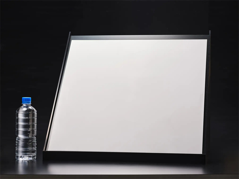
On January 15, 2025, Japan's Nippon Electric Glass Co., Ltd. (NEG) unveiled a new glass-ceramic core substrate, the "GC Core," designed for next-generation semiconductor packaging. With a large panel size of 515×510 mm, this innovative substrate aims to meet the growing demand for larger substrates in the production of advanced semiconductor packages.
Previously, NEG had developed a 300mm square GC Core substrate made from a composite of glass and ceramic powders, which was introduced in June 2024. Building on this, the company has now expanded its capabilities by producing a larger 515×510 mm GC Core substrate, measuring just 1.0mm in thickness. This new development is a significant step forward for the semiconductor industry, where large substrates are increasingly required for packaging larger and more powerful chips, such as those used in data centers and AI technologies.

The GC Core substrate is compatible with widely-used CO2 laser processing machines, enabling fast and crack-free hole drilling. This feature significantly improves mass production efficiency, while keeping manufacturing costs low. Moreover, it allows semiconductor manufacturers to use their existing equipment, reducing the need for expensive new investments.
NEG plans to showcase this large GC Core substrate at the 39th Nepcon Japan exhibition at Tokyo Big Sight, from January 22 to 24, 2025. The product promises to help drive the mass production of next-generation semiconductor packages, a crucial development for the ongoing evolution of the semiconductor industry.
In the context of the growing performance demands of semiconductor devices, the development of the GC Core is positioned as a response to the need for chiplet-based packaging, where multiple chips are placed in a single package. By enabling more efficient use of larger chips, NEG's innovation could play a vital role in the advancement of future semiconductor technologies.
+86 191 9627 2716
+86 181 7379 0595
8:30 a.m. to 5:30 p.m., Monday to Friday
