
-advertisement-

According to Nikkei News, Japanese Prime Minister Fumio Kishida on July 24 visited Rapidus, a startup wafer foundry in Hokkaido. Kishida pledged national financial support for Rapidus' 2nm chip production project through new legislation. The Japanese government considers the plant crucial for enabling the country to manufacture chips at advanced nodes.
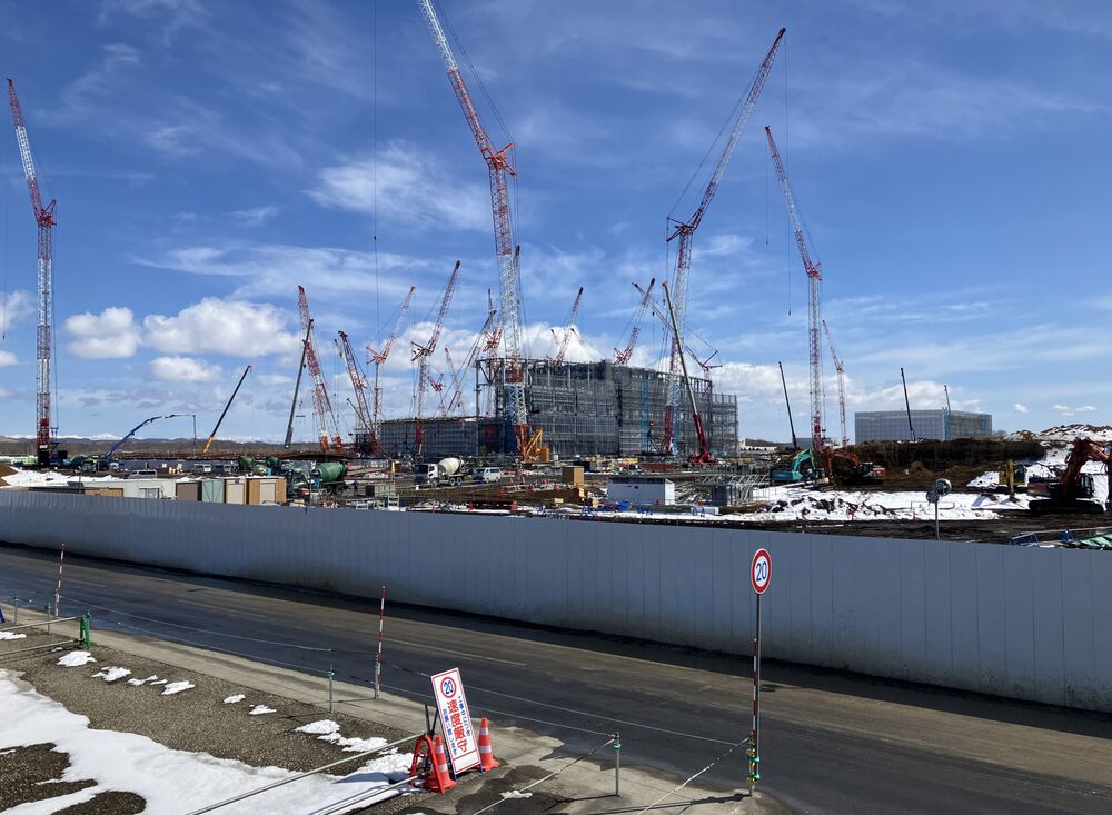
Rapidus is building its advanced chip plant at this site in Chitose, Japan
Rapidus plans to build an advanced wafer fab in Hokkaido by 2027, providing 2nm process technology and advanced packaging. The first phase is expected to cost 5 trillion yen ($32 billion). The second phase, which will commence after 2027, will produce chips using 1.4nm process technology.
So far, the government has approved subsidies of up to 920 billion yen for Rapidus. The company has also secured 7.3 billion yen from investors, including major companies like Toyota and Sony. Despite Mitsubishi UFJ Financial Group's involvement, other large banks remain hesitant to offer loans without government guarantees.
The proposed legislation aims to secure private sector financing for Rapidus through state guarantees. The bill is expected to be introduced in a special legislative session this fall. The government anticipates that the new law will streamline Rapidus' financing process.
"We will promptly submit a bill to the National Diet for the mass production of next-generation semiconductors," said Prime Minister Kishida. "Relevant agencies will begin considering the substantive content of the bill and its submission timeline. We will provide substantial, planned, and targeted investment support for mass production and R&D over multiple fiscal years."
Currently, the lack of large-scale loans, which typically come in the form of syndicated loans, complicates financing due to the need for government guarantees. According to Nikkei News, bank executives are concerned about lending to Rapidus because the company lacks commitments from potential customers and has no proven track record in mass production. Competing with TSMC, Intel Foundry Services, and Samsung Foundry will be challenging, making financing this project risky.
It is estimated that the economic impact of establishing a semiconductor industry in Hokkaido will exceed 18 trillion yen by 2036. Thus, government support for this project is justified, as it is crucial for Japan's national economic security and its domestic semiconductor supply chain.
Editor:Lulu
▼▼▼
Kyushu's semiconductor boom: TSMC investments ignite over 100 projects on Japan's
Intel suspended investment in French and Italian chip plants
Nvidia developing flagship AI chip for Chinese market
+86 191 9627 2716
+86 181 7379 0595
8:30 a.m. to 5:30 p.m., Monday to Friday

