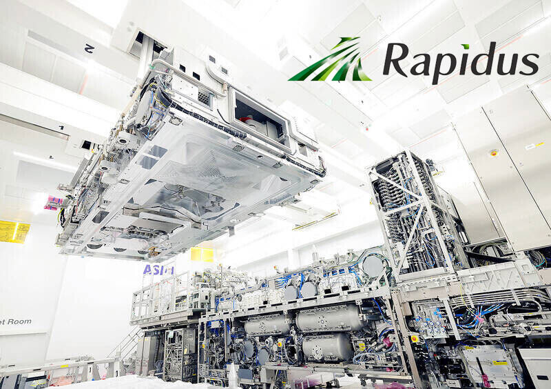
Japan has reached a major milestone in its efforts to revive its semiconductor industry with the installation of its first extreme ultraviolet (EUV) lithography system, a critical tool for the production of advanced 2nm chips. Rapidus, a Japanese semiconductor startup, has begun setting up the ASML Twinscan NXE:3800E EUV lithography system at its Innovative Integration for Manufacturing (IIM-1) facility in Chitose, Hokkaido. This marks Japan’s first acquisition of such a high-tech machine, which is designed for producing cutting-edge logic chips using 2nm process technology.
The system, which weighs 71 tonnes and stands 3.4 meters tall, is being installed in stages, with completion expected by the end of December. Once operational in 2025, the IIM-1 plant will begin producing prototype 2nm chips, and full-scale production is set to begin in 2027. Rapidus plans to develop advanced semiconductor manufacturing capabilities that will contribute to Japan’s goal of achieving ¥15 trillion in semiconductor sales by 2030. This goal is part of a broader national strategy to reduce Japan's dependence on foreign chip imports.

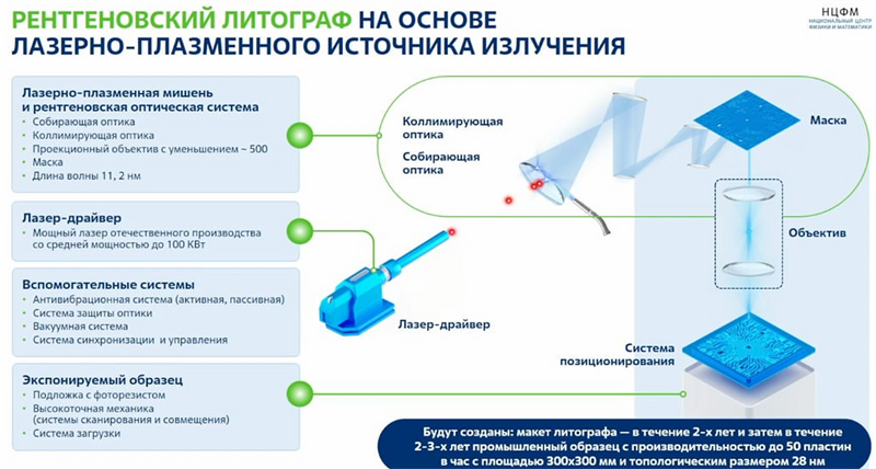
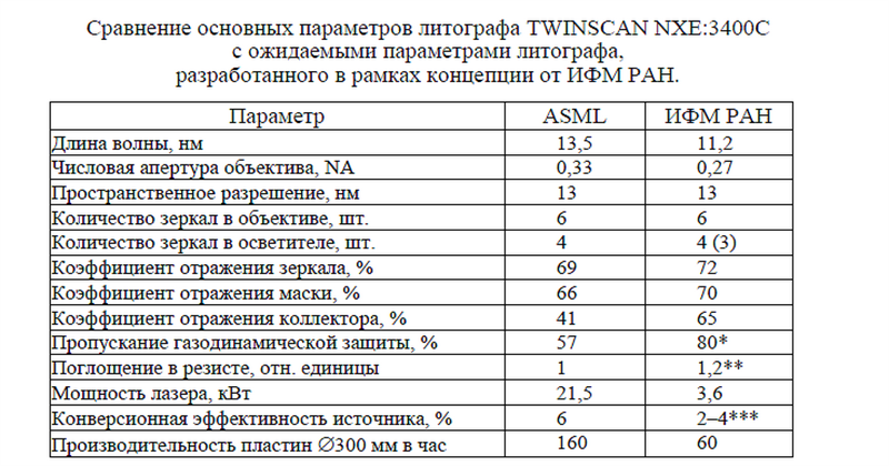
While Japan moves forward with ASML’s EUV technology, Russia is also making strides in the EUV lithography field, albeit with an ambitious and cost-conscious approach. The Russian government has announced plans to develop its own EUV lithography systems, which would use a shorter 11.2 nm wavelength, as opposed to the 13.5 nm wavelength used by ASML. This new wavelength could offer significant advantages, including improved resolution by 20%, reduced optical component costs, and better performance with silicon-based photoresists. Additionally, it promises to reduce contamination of optical elements, extending the lifespan of critical parts like collectors and pellicles.

However, this shift comes with its own challenges. Russia's EUV machines will have lower throughput than ASML’s systems, processing wafers at only about 37% of the speed of current machines. As a result, these systems would be more suited for small-scale production rather than large-volume manufacturing. Moreover, the move to a new wavelength requires a complete redesign of nearly every optical element and recalibration of other processes, including resist chemistry and contamination control.

The Russian development project is expected to take several years, with a timeline of over a decade for the new systems to become commercially viable. Despite these challenges, Russia’s efforts could introduce a new, cost-effective alternative to ASML’s EUV systems, adding a competitive dimension to the global lithography market. The project, led by Nikolay Chkhalo from the Russian Academy of Sciences, is being pursued with the goal of reducing Russia’s reliance on foreign semiconductor technologies.
As both countries push forward with EUV advancements, Japan's focus remains on re-establishing its position in the global semiconductor market with cutting-edge tools from ASML, while Russia seeks to innovate with its own, more affordable EUV solutions. The outcomes of these initiatives could reshape the competitive landscape of semiconductor manufacturing in the coming decade.
+86 191 9627 2716
+86 181 7379 0595
8:30 a.m. to 5:30 p.m., Monday to Friday
