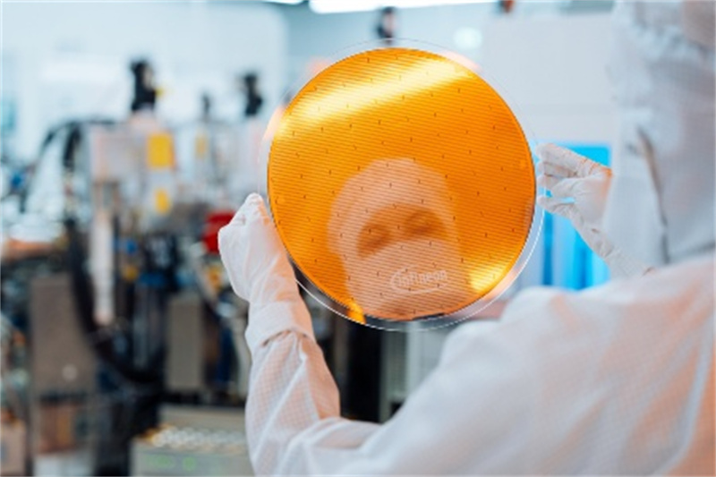
On Oct. 29, Infineon Technologies AG (FSE: IFX / OTCQX: IFNNY) has announced a breakthrough in semiconductor technology by developing the world's thinnest silicon power wafer, measuring just 20 micrometers thick and 300 millimeters in diameter. This ultra-thin wafer, only a quarter the thickness of a human hair, demonstrates Infineon's ongoing commitment to advancing power semiconductor solutions for applications such as AI, data centers, and motor control.
"The world's thinnest silicon wafer reflects our dedication to pushing the limits of power semiconductor technology and advancing energy efficiency," said Infineon CEO Jochen Hanebeck. "This achievement, combined with our capabilities in silicon, silicon carbide (SiC), and gallium nitride (GaN), solidifies our leadership in semiconductor innovation for a decarbonized, digital future."
The innovation will enhance energy efficiency, power density, and reliability across multiple applications. The ultra-thin wafer technology reduces substrate resistance by 50%, translating to over 15% reduction in power loss, especially crucial in AI server power conversion where high current levels are required to bring voltages from 230 V down to under 1.8 V. The new wafer design, leveraging vertical Trench MOSFET technology, enables close AI chip-to-power source connections, minimizing energy loss.

Adam White, Division President of Power & Sensor Systems at Infineon, emphasized the significance: "As AI data centers see rising energy demands, our ultra-thin wafer technology will power AI server configurations efficiently from grid to core. With high growth rates, we anticipate our AI-driven business to reach €1 billion within two years."

Developing this wafer required overcoming substantial technical challenges. Infineon introduced an advanced wafer grinding technique to manage wafer bowing and separation issues, and the thin structure allows seamless integration into existing production lines without added complexity, ensuring high yield and supply security.
Already qualified for use in Infineon's DC-DC converter systems, the new technology is being delivered to initial customers, marking the beginning of a transition to replace conventional silicon wafers over the next three to four years. With a robust patent portfolio backing this innovation, Infineon strengthens its leading position in the semiconductor market with the widest range of silicon, SiC, and GaN technologies, driving the global push toward decarbonization and digital transformation.
+86 191 9627 2716
+86 181 7379 0595
8:30 a.m. to 5:30 p.m., Monday to Friday
