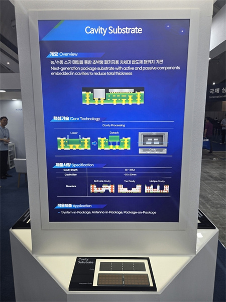
Leading printed circuit board (PCB) manufacturer Simmtech (222800.KQ) has developed a cavity substrate technology, a next-generation ultra-thin semiconductor substrate expected to be widely used in smartphone packaging. With this thinner substrate, Simmtech aims to penetrate the smartphone packaging market.
According to industry reports on the 11th, Simmtech has completed the development of cavity substrates for Package-on-Package (PoP) and Antenna-in-Package (AiP) applications and is currently collaborating with partners for evaluations.
Cavity technology uses lasers to carve out spaces in the substrate where components are embedded, reducing thickness. This makes it ideal for mobile packaging, where minimizing chip size in small form factors is essential.

PoP is commonly used in mobile products for 3D stacking, involving a Flip Chip Ball Grid Array (FCBGA) at the base, with additional FCBGAs, interposers, and memory stacked on top.
Simmtech has developed a cavity interposer that connects the substrate and die within the package. The company has also completed AiP cavity technology, which reduces the thickness of packaging for 5G smartphones.
A company representative noted, "Using a cavity design for the interposer helps reduce the overall height of the package."

-advertisement-
Interest in cavity technology is growing, particularly for PoP and antenna packages. Some smartphone manufacturers are exploring solutions that eliminate the need for sockets altogether.
Cavity substrates are seen as critical to addressing trends in semiconductor packaging, including multifunctionality and high integration. Other industry leaders, such as Samsung Electro-Mechanics and Daeduck Electronics, are also advancing cavity technology development.
Simmtech emphasized that its cavity substrates have fewer material limitations compared to competitors, offering greater flexibility. The company further explained that its process, which involves cutting only the outer portion of the substrate and etching the bottom, is more cost- and time-efficient, and supports the use of various materials.

The company is working with several clients who are evaluating the technology, which can be applied in multiple configurations, including double-sided, multi-tiered, and both-side setups.
Beyond the mobile packaging market, Simmtech is accelerating the development of glass substrates for high-performance computing (HPC).
"We’re currently working on a core glass substrate technology project and will evaluate it in high-density products like flip-chip substrates once it’s ready," a company representative said. "However, challenges remain with glass substrates, particularly in cracking and handling, which will take more time to resolve."
+86 191 9627 2716
+86 181 7379 0595
8:30 a.m. to 5:30 p.m., Monday to Friday
