-advertisement-
As applications in AI, high-performance computing (HPC), and big data drive innovation, glass substrates in semiconductor packaging are gaining attention. However, several technical challenges must be addressed for their commercialization.
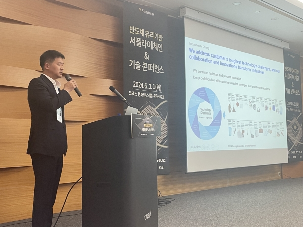
During the "Semiconductor Glass Substrate Supply Chain & Innovation Technology" conference held in Seoul on June 11, Dr. Junro Yoon of Corning highlighted both the issues and potential solutions for glass core packages. Glass substrates offer smoother surfaces and lower signal loss compared to organic silicon, in addition to increased heat resistance. Yet, addressing the brittleness of glass, developing suitable packaging materials and equipment, and advancing glass metallization processes are critical hurdles.
Corning proposes that restructuring the supply chain and investing in new equipment and facilities could pave the way for commercialization, which is expected between 2026 and 2030.
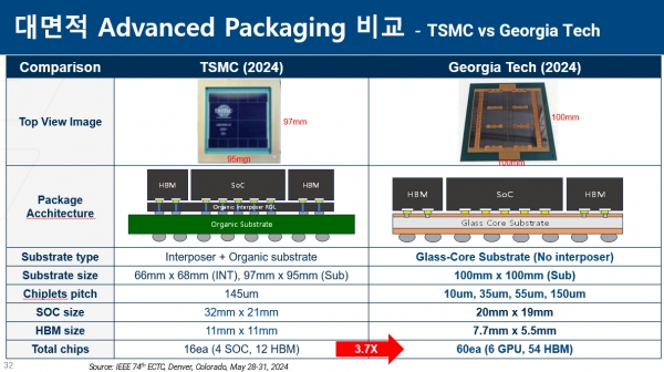
Professor Yong-Won Lee of Georgia Tech, speaking at the same conference, noted that if glass substrates become commercialized, advanced packaging technologies like TSMC's 2.5D CoWoS would face significant threats. Unlike traditional plastic cores, glass substrates offer reduced delamination and better interconnect and die crack resistance. The industry expects that mass production of package substrates larger than 100x100mm will be feasible.
Recently, Georgia Tech presented research results at the ECTC, demonstrating the mounting of 60 chips (6 xPUs and 54 HBMs) on a glass substrate. Compared to TSMC's CoWoS-R, which was unveiled at the same conference, the number of chips mounted increased by 3.7 times. Professor Lee explained, "Glass substrates offer relative freedom in terms of chiplet pitch and size, allowing for an increase in the number of chips that can be mounted."
Leading companies such as Intel, Absolics, Samsung Electro-Mechanics, Dai Nippon Printing (DNP), and Ibiden are at the forefront of pushing for commercialization. Among these, Absolics, a joint venture between SKC and Applied Materials (Applied), has recently completed the Covington glass substrate plant in Georgia and has started trial operations. Mass production is scheduled for the first half of next year. However, Professor Lee has also warned of potential competition from Chinese firms, which could impact the competitive edge of Korean companies.
In summary, while glass substrates in semiconductor packaging present promising advantages, the path to commercialization is paved with challenges that require substantial investment and innovation in technology and the supply chain.
Editor:Lulu
▼▼▼
Aimtron Electronic Ltd., has recently gone public!
Haesung DS leads the way in supply price linkage, honored as 2023 Outstanding Company
Rogers announces further actions to streamline operations and drive margin improvement
MacroFab announces the offering of custom PCBs to provide even more custom options to customers
Burkle to equip TTM's Malaysian PCB facility with 28 presses
FTG has signed a contract worth $17 million CAD with Shanghai Avionics Company Ltd (SAVIC)
+86 191 9627 2716
+86 181 7379 0595
8:30 a.m. to 5:30 p.m., Monday to Friday

