May 10th(PCB UNION)——Kang Hae-chul, CEO of Gigavis, announced during an Investor Relations Meeting prior to the company's listing on the KOSDAQ market, that the company has developed a new device that can reduce the circuit detection line width of semiconductor substrates to 2 microns, and this device will be launched globally for the first time this year. In addition, they are also researching a device that can repair circuits with a line width of up to 3 microns, with the goal of launching it in 2025.
Gigavis predicts that it will benefit from the growth of the next-generation semiconductor substrate flip chip ball grid array (FCBGA) market. Packaging substrates connect semiconductor chips to the main substrate to transmit electrical signals and protect semiconductors from external impacts. General packaging substrates are used in mobile devices such as smartphones, while FCBGA is mainly loaded onto high-performance central processing units (CPU) and graphics processing units (GPU) in computers (PCs), servers, and networks. Well-known companies such as Samsung Electronics, LG Innotek, Daejeon Electronics are investing heavily in FCBGA. As Kang Hae-chul put it "high-performance boards are larger in size but have smaller circuits, so they require more accurate inspection and maintenance than ordinary boards."
According to PCB UNION, Gigavis' operating profit last year was KRW 43.9 billion, an increase of 176% from the previous year, with sales increasing by 127% to KRW 99.7 billion. Since 2020, the operating profit margin has remained above 35%, and as of the end of last year, the order backlog was KRW 122.8 billion.
More information about Gigavis from PCB NUNION:Gigavis will be listed on the KOSDAQ on May 15

Establishment in 2004,GigaVis has been vigorously developing, supplying optical inspection tools, laser applications, In-line tools to the semiconductor, PCB, and battery industries and it aims to be the most advanced AOI company in the world. Since the start of research and development of Optics, more than 1500 sets of AOI and AFVI have been successfully installed and operated by our customers. GigaVis’s global competitiveness is underpinned by the metrology based algorithm that is in conjunction with decades of field experience.
Gigavis is currently supplying world-class semiconductor packaging substrate manufacturers, including Samsung Electronics, LG Innotek, and Daeduck Electronics in South Korea, Ibiden and Shinko Denki in Japan, as well as Unimicron and Nanya in Taiwan, China.
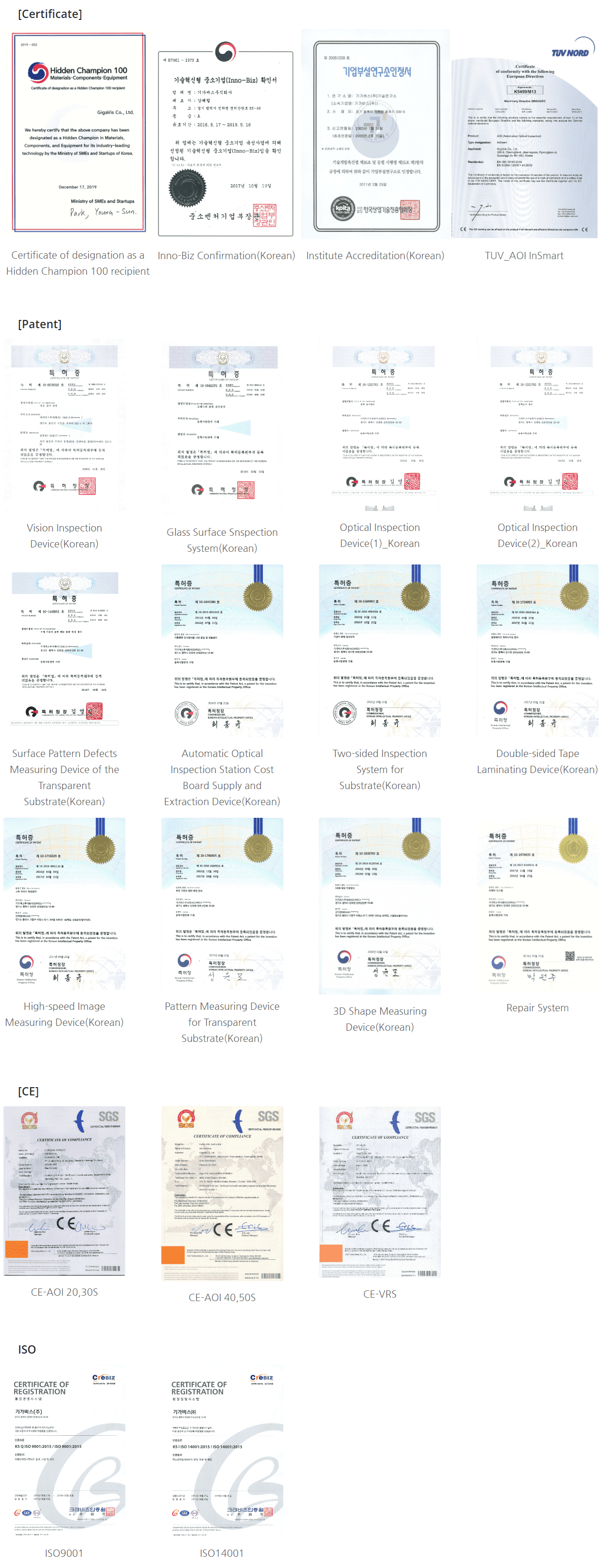
Patent Certificate of Gigavis

+86 191 9627 2716
+86 181 7379 0595
8:30 a.m. to 5:30 p.m., Monday to Friday
