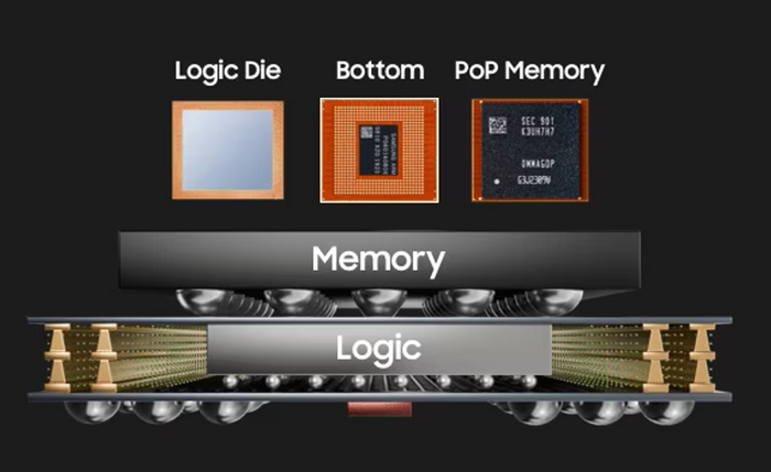
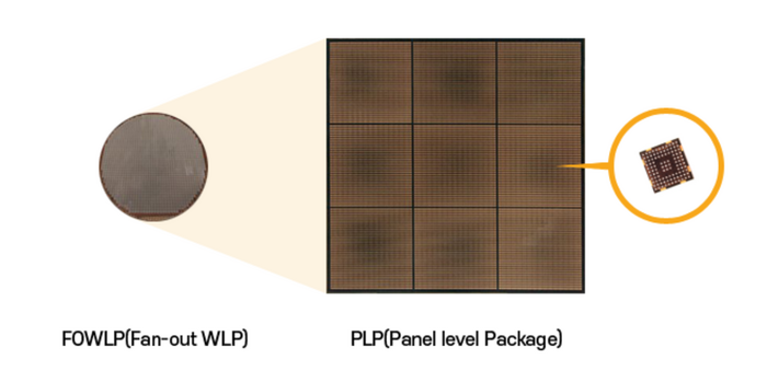
As fan-out panel-level packaging (FOPLP) technologies gain traction in advanced chip manufacturing, the PCB industry is positioned to play a pivotal role in supporting this next-generation innovation. Global semiconductor leaders Samsung and TSMC are pursuing distinct paths for FOPLP materials, opening doors for PCB manufacturers to adapt and thrive in this evolving landscape.
FOPLP: A Game-Changer for PCB Applications
FOPLP replaces traditional circular wafers with rectangular panels, significantly improving chip yield and reducing material waste. This shift enables more efficient manufacturing processes and aligns with the growing demand for high-performance chips in artificial intelligence (AI) applications. The technology's reliance on advanced substrate materials creates new opportunities for PCB suppliers.
Material Divergence:Organic vs. Glass
Samsung is doubling down on organic substrates, a proven material widely used in PCB manufacturing. organic panels are cost-effective, flexible, and supported by established production processes. Samsung’s expertise in PCB-based packaging technologies strengthens its position as it continues to refine FOPLP solutions.
On the other hand, TSMC is exploring glass substrates, valued for their superior thermal stability and flatness. These properties are expected to support tighter interconnect spacing and enhanced chip performance, though glass introduces higher manufacturing complexity. TSMC’s move toward glass panels could redefine material requirements for PCB partners supporting advanced packaging.

Opportunities for PCB Manufacturers
The divergence in material strategies highlights the need for PCB manufacturers to innovate and align with industry trends. The increasing demand for precise substrates, whether organic or glass, underscores the importance of material and process innovation within the PCB sector. Companies specializing in advanced panel materials or custom solutions may find themselves well-positioned to capture new market opportunities.

Collaboration and Adaptation
To meet the growing needs of semiconductor giants, PCB suppliers will need to collaborate closely with chipmakers and invest in technologies that align with FOPLP requirements. This includes adapting production lines to accommodate larger panel sizes, enhancing surface uniformity, and ensuring compatibility with cutting-edge interconnect designs.

A Transformative Period for the Industry
As FOPLP adoption accelerates, the PCB industry’s role in supporting this technological shift will only grow. By embracing these changes and collaborating across the semiconductor supply chain, PCB manufacturers can position themselves at the forefront of the next wave of chip packaging innovations.
This new era in chip packaging not only underscores the synergy between PCB technology and semiconductor advancements but also points to a promising future for material and design innovations in the PCB sector.
+86 191 9627 2716
+86 181 7379 0595
8:30 a.m. to 5:30 p.m., Monday to Friday
