A leading innovator in inkjet printing technology, Elephantech announced on December 17, 2024, that it has successfully developed a general-purpose multilayer PCB using its proprietary inkjet printing technology, reducing copper usage by 70-80%. This marks a significant milestone, as general-purpose multilayer PCBs account for 80% of the global PCB market. The company estimates this innovation could reduce global PCB manufacturing costs by over ¥1 trillion (about $6.39 billion or 47.4 billion yuan) annually. Prototype deliveries are set to begin in early 2025.
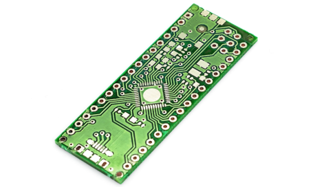
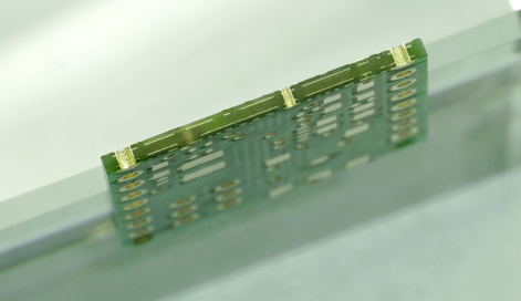
Unlike traditional PCB manufacturing, which involves etching away unnecessary copper, Elephantech’s method prints metal only where needed and grows copper via electroplating. This approach significantly reduces copper consumption, water usage, and CO2 emissions.
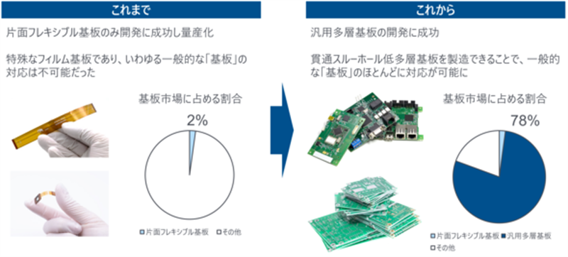
Previously, Elephantech only produced single-sided flexible PCBs, which make up 2% of the global market. However, breakthroughs in rigid substrate adhesion and multilayer compatibility have enabled the early development of multilayer PCBs, initially planned for 2027. The company believes this technology could replace most standard PCBs used in electronics, especially six-layer or fewer rigid boards, which dominate the market.
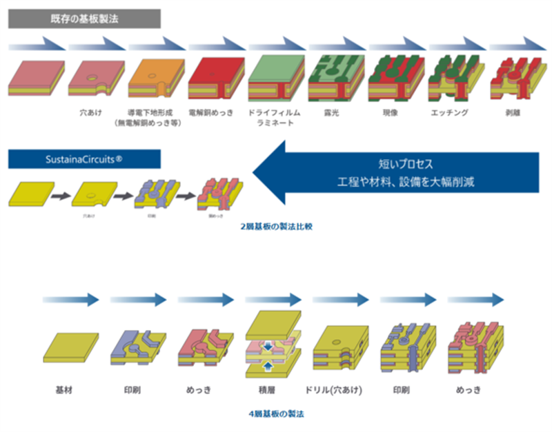
Elephantech highlights that multilayer PCBs consume more copper due to multiple layers of foil and through-hole plating. Its new process not only cuts material costs but also simplifies manufacturing by simultaneously forming vias and traces.
Innovations Driving Success
Two key advancements enabled this breakthrough:
1.Rigid Substrate Compatibility: A newly developed primer and copper nanoparticle ink ensure strong adhesion to FR-4, the most common rigid PCB material. This new system also withstands high temperatures, meeting industrial standards.
2.Multilayer Compatibility: Improvements in ink application and primer technology allow the formation of multilayer boards, though the process is currently limited to rigid substrates.
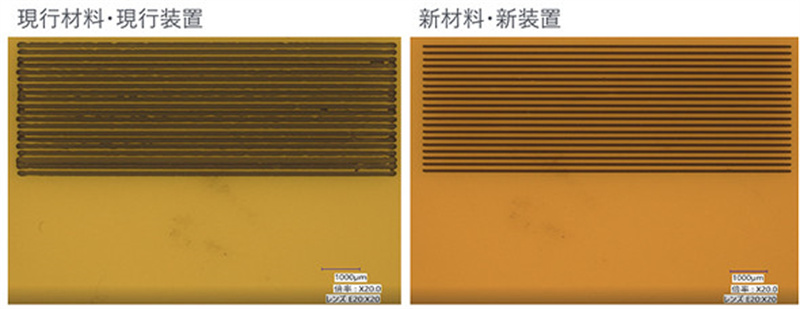
Additionally, Elephantech has achieved finer wiring capabilities, forming traces as narrow as 50/50 µm, compared to the previous 100/100 µm. For high-current applications, the new process supports copper layers up to 100 µm thick, making it suitable for power electronics.

A Cost-Effective, Scalable Solution
Elephantech is working with several electronics manufacturers and plans to provide prototypes in 2025. The company’s method can integrate into existing PCB factories by adding its printing equipment to standard production lines, minimizing infrastructure changes.
With copper prices rising, Elephantech’s selective plating approach becomes increasingly economical, offering a sustainable and cost-effective alternative for global PCB production. This innovation positions the company as a key player in reshaping the industry toward greener and more efficient manufacturing.
+86 191 9627 2716
+86 181 7379 0595
8:30 a.m. to 5:30 p.m., Monday to Friday
