
-advertisement-

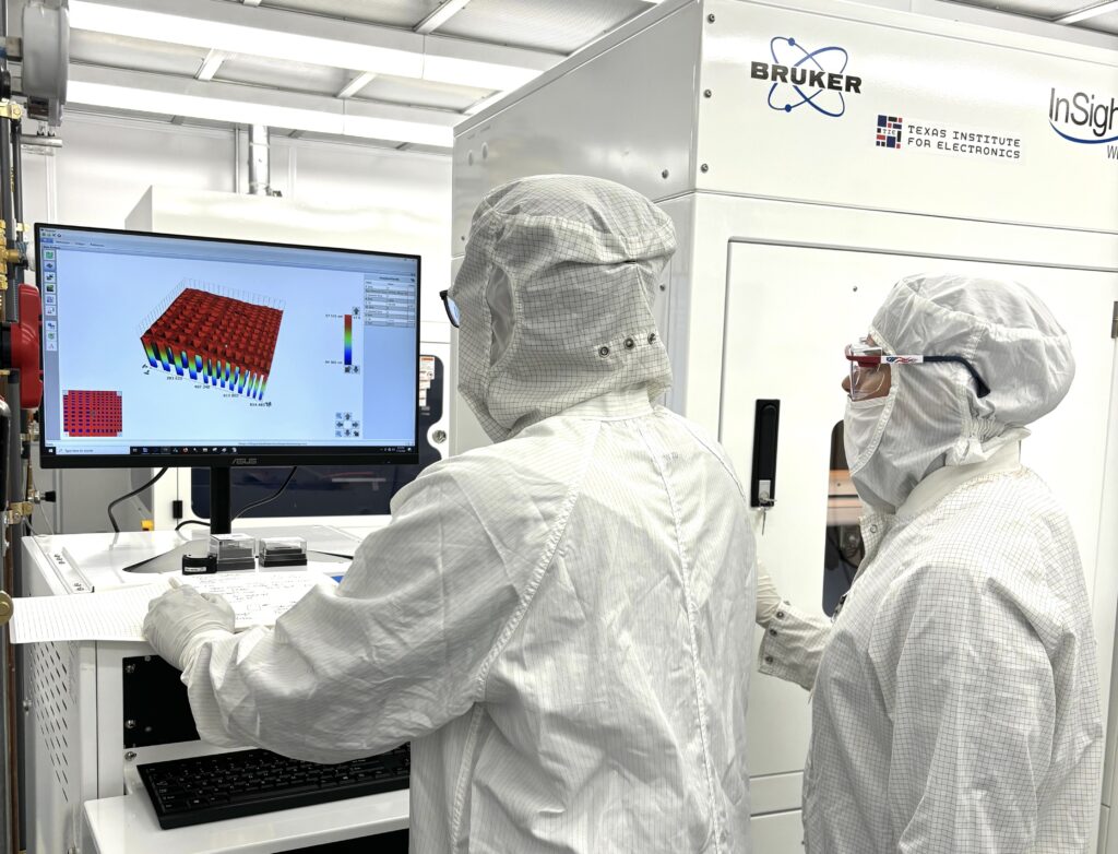
The Defense Advanced Research Projects Agency (DARPA) has chosen the Texas Institute for Electronics (TIE) at The University of Texas (UT) at Austin to create 3D-integrated multi-chiplet advanced semiconductor microsystems for the U.S. Department of Defense. This project includes establishing a national R&D and prototyping facility to produce high-performance, energy-efficient, lightweight, and compact defense systems.
A $1.4 Billion Project
Part of DARPA's Next Generation Microelectronics Manufacturing (NGMM) program, the project aims to design 3D packaging technologies and build facilities for both military and civilian use. It involves a $1.4 billion investment, with DARPA contributing $840 million and the Texas Legislature adding $552 million to TIE.
This funding will modernize two UT fabrication facilities to support dual-use innovations in 3DHI multi-chiplet integration for the defense and semiconductor industries. These facilities will be self-sustaining and accessible to academia, industry (including startups), and government.
Project Phases
The program spans two phases, each lasting 2.5 years. In the first phase, TIE will develop the center's infrastructure and foundational capabilities. The second phase will involve creating 3D-integrated (3DHI) hardware prototypes crucial to the DoC and automating various processes. TIE will also collaborate with DARPA on other design challenges.
Securing the Supply Chain
"By investing in leading-edge microelectronics manufacturing, we are helping secure this vulnerable supply chain, boosting our national security and global competitiveness, and driving innovation in critical technologies," said U.S. Sen. John Cornyn. "The next generation of high-performing semiconductors these resources will enable through DARPA's partnership with UT TIE will help bolster our defense and pave the way for the U.S. to reclaim its leadership role in this critical industry."
Military-Grade 3D Packaging
Modern military applications rely on several discrete chips, which complicates systems and increases costs. This project aims to build multi-chiplet designs integrating different logic into one compact package, enabling smaller, lighter military devices.
While process technologies from companies like Intel, GlobalFoundries, or TSMC are sufficient for many applications, aerospace and military demands often require more specialized technologies. DARPA's NGMM program, introduced in late 2023, addresses these needs by developing aerospace and military-grade packaging technologies.
Summary
This project will enhance U.S. national security and global military leadership by developing sophisticated multi-chiplet processors. The labs and manufacturing capabilities in Texas will also be available to developers and producers of civilian applications, boosting scientific innovation and industrial strength in the USA.
Editor:Lulu
▼▼▼
OpenAI and Broadcom in talks about developing new AI chip
Vietnam partners with U.S. firms to train 50,000 semiconductor engineers by 2030
Intel builds brand-new interactive experience to showcase AI at Paris Olympics
Taiwan chip firm GlobalWafers wins $400m for US factories
AMD and IIT-B join hands to support semiconductor startups in India
MediaTek develops Arm-based server chips with TSMC's 3nm process
+86 191 9627 2716
+86 181 7379 0595
8:30 a.m. to 5:30 p.m., Monday to Friday

