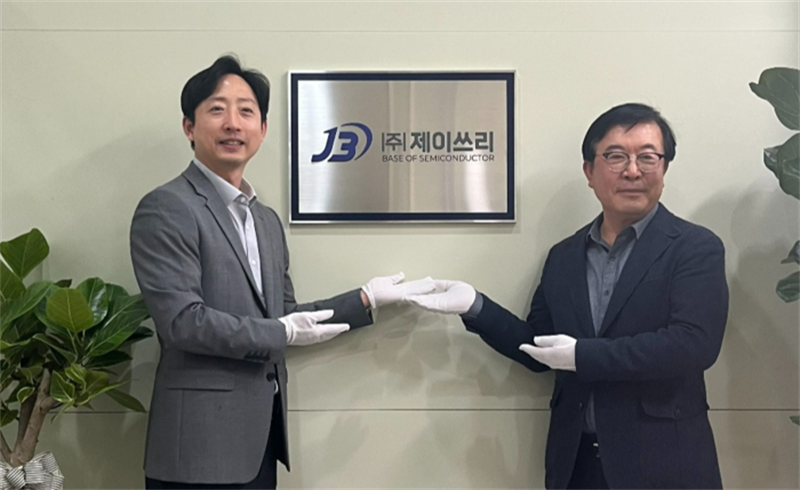
J3, a semiconductor wafer recycling company recently acquired by Chemtronics (KOSDAQ: 089010) subsidiary Regenics, unveiled its new corporate identity (CI) on March 28th, highlighting its innovative vision and leadership in the wafer industry.
The new CI features a stylized ‘J' with a line forming the number ‘1,' symbolizing the company's ambition to lead the industry. The sweeping curve extending from the ‘J' represents the shape of a wafer and the company's determination to expand into the global market. A blue color scheme emphasizes professionalism and reliability, reinforcing its global corporate image.
Chemtronics acquired J3 through Regenics last month to strengthen its semiconductor materials business and create synergy in its emerging glass substrate sector.
Chemtronics CEO Kim Eung-soo stated, "By combining our expertise in high-purity semiconductor materials and Through-Glass Via (TGV) technology with J3's ultra-precision planarization capabilities, we aim to advance glass substrate technology." He also emphasized plans to enhance manufacturing competitiveness by securing advanced infrastructure, including hydrofluoric acid-approved factory zones, wastewater treatment facilities, and chemical mechanical polishing (CMP) equipment.

J3 specializes in the recycling of 6-inch, 8-inch, and 12-inch semiconductor wafers, utilizing both chemical and physical regeneration processes. Its ultra-precision planarization and fine particle control technology have made it a key partner for major semiconductor companies such as Samsung Electronics and SK Hynix.
Chemtronics anticipates significant synergy from the acquisition, leveraging J3's infrastructure and expertise in glass substrate development. A company representative added, "We will focus on developing glass substrate technology by integrating our high-purity semiconductor material technology and TGV processing with J3's precision planarization capabilities."
+86 191 9627 2716
+86 181 7379 0595
8:30 a.m. to 5:30 p.m., Monday to Friday
