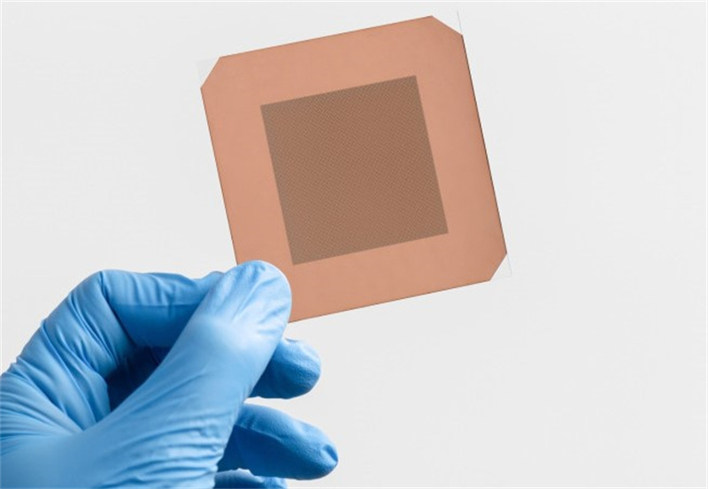
C&G Hi Tech (264660.KQ), a leading technology company in the PCB (printed circuit board) sector, has successfully applied a new physical vapor deposition (PVD) technique to form copper thin films on the walls of through-glass vias (TGV) in next-generation glass substrate. This breakthrough addresses a significant technical challenge by ensuring uniform copper thin film deposition within vias with an aspect ratio of up to 1:10 (hole diameter to depth).
According to a company spokesperson, C&G Hi Tech's self-developed M-PVD (Magnetron-PVD) method efficiently transfers metal atoms to the walls of the vias by controlling their energy. This approach can replace traditional chemical electroless plating and electroplating processes, providing a more efficient and eco-friendly solution.
The spokesperson further explained that while traditional PVD processes, such as DC sputtering, offer environmental benefits and high-crystallinity thin films, they struggle to maintain uniform deposition in complex structures. In contrast, M-PVD technology can achieve consistent copper thin films even in vias with an aspect ratio exceeding 1:10, making it a revolutionary advancement for glass substrate manufacturing.
C&G Hi Tech's core technology features two major advantages:
● Strong adhesion between copper and glass achieved through ion beam surface treatment
● M-PVD process for metal deposition on complex via walls
These innovations also solve environmental and cost challenges associated with conventional processes, such as the use of toxic chemicals and process instability. The company's technology offers a solution that reduces environmental pollution and manufacturing costs while improving process stability and reproducibility, making it a game-changer for high-density PCB manufacturers.

The successful copper thin film formation with excellent adhesion to glass offers a promising future for multi-layer glass substrate development. PCB manufacturers developing high-density PCBs using traditional wet-chemical processes stand to benefit from simplified subsequent processes and reduced costs.
C&G Hi Tech has already achieved copper-glass adhesion strength exceeding 7N/cm and successfully scaled the process for large-area applications with an aspect ratio of 1:5. The company is currently establishing mass production systems and plans to showcase this advanced glass substrate technology at SEMICON KOREA 2025, held from February 19-21 at COEX, Seoul.
Leveraging its patented core technology, C&G Hi Tech is expanding its cooperation with domestic and international industrial enterprises, research institutions, and academic organizations. The company is not only focused on next-generation glass substrate but also exploring applications in industries such as displays, energy storage, 5G/6G telecommunications, and high-value decorative glass.
A company representative stated, "Through continuous development of new products and international partnerships, we aim to solidify our position in the domestic and global next-generation Glass Substrate industry and grow as a technology-driven industry leader."
+86 191 9627 2716
+86 181 7379 0595
8:30 a.m. to 5:30 p.m., Monday to Friday
