
-advertisement-
TSMC’s fan-out (InFO) packaging process will no longer be exclusively used by Apple. According to a report from Commercial Times, it’s revealed that Google’s self-developed Tensor chips for their phones will switch to TSMC’s 3nm process next year and will also start using InFO packaging.
TSMC developed InFO packaging based on FOWLP (fan-out wafer-level packaging), which gained prominence after being adopted by the A10 processor in the iPhone 7 in 2016.
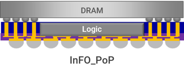
TSMC indicated that the current InFO_PoP technology has advanced to its ninth generation. Last year, it successfully certified 3nm chips, achieving higher efficiency and lower power consumption for mobile devices. The InFO_PoP technology, which features a backside redistribution layer (RDL), has entered mass production this year.
Google will shift to TSMC for the Tensor G5 chips, which will be used in the Pixel 10 series next year. These chips will not only utilize the 3nm process but will also adopt integrated fan-out packaging.
This year’s Tensor G4 chips, set to be announced soon, use Samsung’s FOPLP (fan-out panel-level packaging). Although wafer-level packaging (WLP) is generally considered to have advantages over panel-level packaging (PLP), FOWLP still prevails at this stage due to yield and cost considerations.
TSMC has also begun developing FOPLP technology. Previously, per sources cited by a report from MoneyDJ, TSMC has officially formed a team, currently in the “Pathfinding” phase, and is planning to establish a mini line with a clear goal of advancing beyond traditional methods.
Although it is not expected to mature within the next three years, major customers like NVIDIA have partnered with foundry companies to develop new materials. One of TSMC’s major clients has already provided specifications for using glass materials.
Traditionally, chip advancements have been achieved through more advanced process nodes. However, new materials could enable the integration of more transistors on a single chip, achieving the same goal of scaling.
For instance, Intel plans to use glass substrates by 2030, potentially allowing a single chip to house one trillion transistors – 50 times the number in Apple’s A17 Pro processor. This suggests that glass substrates could become a significant milestone in chip development.
Editor:Vicky
▼▼▼
Tata Group's new semiconductor plant to produce 48.3 million chips daily, creating 27,000 jobs
Kioxia announces completion of new flash memory manufacturing building in Kitakami Plant
Taiwan' s ASE considers building fab in Kyushu
Infineon sells two backend manufacturing sites to ASE
AI chipmaker Cerebras confidentially files for US IPO
Belgian semiconductor makers declared bankrupt, over 400 jobs at risk
+86 191 9627 2716
+86 181 7379 0595
8:30 a.m. to 5:30 p.m., Monday to Friday

