-advertisement-

Atotech Korea, a leading surface treatment company, has launched a project aimed at achieving 2/2μm line/space (L/S) in semiconductor package substrates.
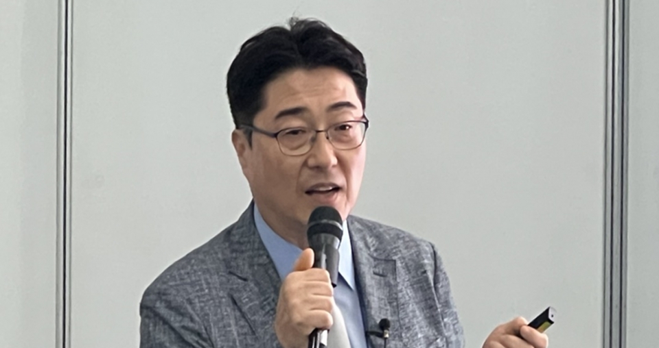
At a technical seminar during the KPCA Show 2024 on September 4, Hong Yoo-sik, Head of Atotech Korea, stated, "The semiconductor package substrate industry is moving toward achieving 2/2μm L/S, and we are currently working on several projects to make this a reality." He added, "Achieving below 2/2μm is challenging for package substrates and may require shifting to semiconductor-level technologies."

Hong Yoo-sik, Head of Atotech Korea, presents at a technical seminar during the KPCA Show in Incheon on September 4
Hong also mentioned that major customers, including Samsung Electronics' semiconductor division, Amkor, Samsung Electro-Mechanics, and LG Innotek, are working on advanced packaging solutions like 2.3D packaging and pushing for L/S to be reduced to 5/5μm and eventually 2/2μm. Atotech is actively participating in these projects.
Hong emphasized, "We are reviewing the chemical solutions and equipment needed to support the transition from 5/5μm, considered the industry limit for package substrates, down to 2/2μm." As the number of I/O terminals in semiconductors increases, the package substrates must implement thinner, denser circuits.
Atotech is particularly focused on via holes, which connect the layers of substrates. As circuit widths shrink, the size of vias must also decrease, requiring advanced equipment to create ultra-small via holes. Hong explained, "Smaller via holes reduce the contact area at the bottom, increasing the risk of cracks. We are addressing this with solutions like copper plating, desmear, chemical copper, and laser technology." He also mentioned ongoing research to enhance reliability in via hole production and expects to present further developments at next year’s KPCA Show.
He noted that packaging technologies have evolved from placing a single semiconductor on a package substrate to supporting multiple semiconductors on one substrate. "The number of I/O terminals has increased significantly, making efficient packaging of multiple semiconductors a key technology."
At the KPCA Show 2024, Atotech Korea showcased several new products, including the eco-friendly Securiganth MV Cleaner GFR-S1, which has secured references from key clients, and Cupraganth MV, which is being evaluated in Japan, Taiwan, and South Korea. The company also promoted its Printoganth MV TP2 and TP3 chemical copper solutions.
Atotech Korea is the South Korean branch of Atotech, a German company specializing in chemical products for PCBs and semiconductors. Atotech was acquired by U.S. semiconductor components company MKS Instruments in 2022 and now operates as part of MKS's Materials Solutions Division under the brand name MKS Atotech.
Editor:Lulu
▼▼▼
'TGV leader' Philoptics expands aggressively into the glass substrate market
HASS embarks on developing key materials for semiconductor packaging
Unitech breaks ground on new HDI PCB manufacturing facility in Thailand's S Industrial Estate
Samsung Electro-Mechanics and LG Innotek unveil next-gen semiconductor substrates at KPCA Show 2024
AT&S Malaysia partners with Universiti Sains Malaysia on copper recycling research
Samsung to provide early payments of KRW 870 Billion to suppliers ahead of Chuseok
+86 191 9627 2716
+86 181 7379 0595
8:30 a.m. to 5:30 p.m., Monday to Friday
