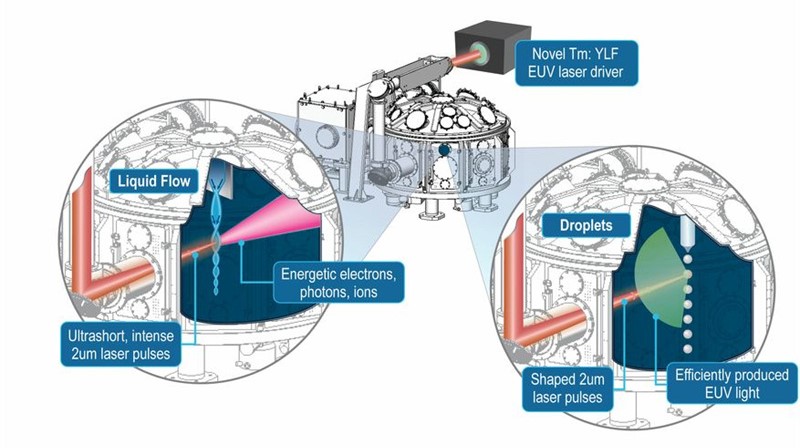
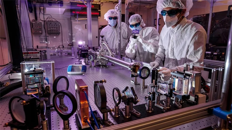
The Lawrence Livermore National Laboratory (LLNL) is spearheading a groundbreaking project that could revolutionize the future of semiconductor manufacturing. Researchers at LLNL are developing a petawatt-class thulium laser, known as the Big Aperture Thulium (BAT) laser, which promises to increase the energy efficiency of extreme ultraviolet (EUV) lithography systems by a factor of ten. This technology, still in its early stages, could eventually replace the current CO2 lasers used in EUV machines, transforming the efficiency of semiconductor production.
EUV lithography, crucial for producing the latest generations of advanced microchips, is an incredibly power-hungry process. Current EUV machines, like those from ASML, consume vast amounts of energy due to their reliance on high-powered CO2 lasers. These lasers are used to create a plasma by vaporizing tin droplets, which in turn emit the 13.5-nanometer light necessary for photolithography. The intense energy required to generate and manipulate this plasma—along with the complex cooling systems—results in power demands exceeding 1,000 kilowatts per machine.
LLNL's BAT laser, which operates at around 2 microns—a wavelength significantly shorter than the 10-micron wavelength used by CO2 lasers—could improve the efficiency of EUV systems by increasing the plasma-to-EUV light conversion. This shift in laser technology, built around thulium-doped yttrium lithium fluoride, could also offer superior electrical efficiency and heat management compared to current gas-based lasers. The laser's solid-state design, powered by diodes rather than gas, allows for higher repetition rates and better energy management.

Over the next four years, a $12 million initiative funded by the Department of Energy (DOE) will explore how the BAT laser can work with EUV light sources. The goal is to demonstrate that the new laser technology can significantly reduce the power consumption of semiconductor fabs while increasing chip manufacturing speeds. This is crucial, as the energy demand of current EUV systems is one of the key concerns for the semiconductor industry, which is projected to use an astonishing 54,000 gigawatts annually by 2030.

The project is part of LLNL's involvement in the Extreme Lithography & Materials Innovation Center (ELMIC), a research initiative under the DOE's Office of Science. Through this partnership, LLNL aims to enhance the basic science behind EUV generation and plasma-based technologies. It brings together scientists from leading institutions, including SLAC National Accelerator Laboratory, ASML, and the Advanced Research Center for Nanolithography (ARCNL), to test the BAT laser's efficiency and potential for scaling.

The BAT laser's development is not just about reducing energy consumption; it could also make “beyond EUV” lithography systems possible—allowing for the creation of smaller, faster, and more powerful chips. If successful, the new laser technology will represent a leap forward in semiconductor fabrication, offering higher precision and efficiency with lower power requirements.
LLNL researchers have already conducted theoretical plasma simulations and proof-of-concept demonstrations over the past five years, laying the groundwork for this new phase of exploration. The team's work has already had a significant impact on the EUV community, and now, with DOE support, they are poised to take the next step in realizing this transformative technology.
As semiconductor manufacturing becomes increasingly energy-intensive, innovations like the BAT laser could help meet the growing demand for more efficient, sustainable production technologies. The project is expected to have a major impact not only on EUV lithography but also on fields like high-energy physics and inertial fusion energy, underscoring the broad potential applications of this advanced laser technology.
In conclusion, while it may take years to fully integrate the BAT laser into semiconductor production, its development is an important step toward creating more energy-efficient EUV systems, offering the possibility of faster, greener, and more cost-effective chip manufacturing for the future.
+86 191 9627 2716
+86 181 7379 0595
8:30 a.m. to 5:30 p.m., Monday to Friday
