
-advertisement-
Aculaser, known for its laser equipment, has officially entered the glass substrate market by establishing a joint venture called ‘AP Solutions.’


On the 14th, Aculaser announced the formation of AP Solutions in partnership with Daichi Korea and DK Tech. Aculaser holds a 51% stake in the new company, while Daichi Korea and DK Tech hold 30% and 19% stakes, respectively. Aculaser’s CEO, Choi Ji-hoon, will also serve as the CEO of AP Solutions.
An Aculaser representative stated, "AP Solutions will focus on developing glass substrate manufacturing technology, related equipment, and material technology sales, as well as providing solutions for manufacturing process optimization." The representative added, "The company plans to establish a glass substrate platform that will allow for technology transfer and process improvement services when necessary." Additionally, design consulting services related to glass substrates will be provided through DK Tech.
The new company plans to supply samples of 240mm x 240mm core glass substrates using direct plating technology to both domestic and international customers, as well as to glass substrate development companies, later this year. By the second quarter of 2025, they also plan to establish a mass production platform for 510mm x 515mm substrates.
AP Solutions’ glass substrate platform features environmentally friendly, glass-compatible material processing. The platform uses a hybrid bonding material developed by Japan’s Daichi Corporation, which ensures strong adhesion between the glass surface and metal materials such as copper (Cu) and nickel (Ni).
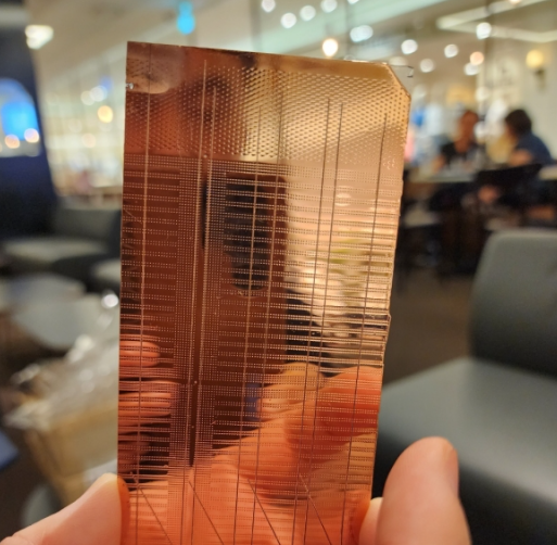
TGV processing with IMB application + Cu plating sample
Through this technology, the company expects to streamline the mass production process, reducing the steps from physical vapor deposition (PVD) for through-glass vias (TGV), glass surface treatment, sputtering (formation of the Cu seed layer), primary electroless Cu plating, secondary electroplating, and post-treatment to a simplified process involving TGV, glass surface treatment, hybrid bonding application, and electroless Cu plating.
Choi Ji-hoon, CEO of Aculaser, commented on the joint venture, saying, "This partnership allows Aculaser to engage in more aggressive and stable business activities, creating strong synergies between the companies and providing new growth momentum for our business."
Editor:Lulu
▼▼▼
LG Innotek struggles to expand in Samsung smartphone CoF market as Stemco leads
STARTEAM GLOBAL adopts Notion Systems'digital n.jet soldermask system
Samsung Electro-Mechanics vs. LG Innotek CEO compensation: Who comes out on top?
Han's CNC reports 102.89% surge in H1 2024 Revenue, driven by strong PCB equipment demand
+86 191 9627 2716
+86 181 7379 0595
8:30 a.m. to 5:30 p.m., Monday to Friday

