Achilles Corporation (Headquarters: Shinjuku, Tokyo; President: Ichiro Hike) has developed a new technology for high-adhesion plating on glass substrates using its proprietary polypyrrole plating method. This innovative technology will be showcased at Achilles' booth at SEMICON Japan 2024.
The company has developed a unique plating technique using conductive polymer polypyrrole, which has allowed them to offer high-adhesion plating solutions for a variety of difficult-to-plate materials. Achilles holds approximately 50 patents related to the polypyrrole plating method. Until now, forming high-adhesion plating films on glass substrates was considered a challenge. However, with this new method, Achilles has successfully developed a technology that creates high-adhesion plating films on glass substrates through a low-temperature, atmospheric-pressure process.

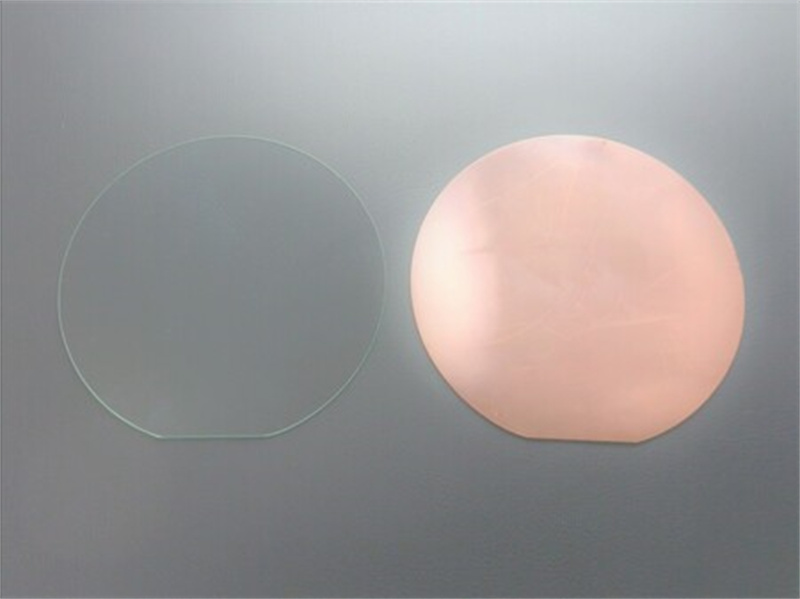
Glass substrate before (left) and after (right) plating treatment
As semiconductor miniaturization and high integration continue to progress, glass is gaining attention as a new material for semiconductor package substrates. Achilles plans to further advance research and development on fine wiring formation and establish mass-production technologies to support the manufacturing of next-generation semiconductors.

Achilles will exhibit at SEMICON Japan 2024, held at Tokyo Big Sight from December 11. At booth number 3242, the company will present the high-adhesion plating technology for glass substrates using the polypyrrole method and showcase samples of fine wiring formations.

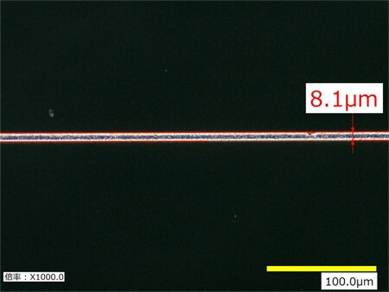
Fine wiring formed on a glass substrate through plating
About the Polypyrrole Plating Method:
The polypyrrole plating method is a plating technology developed by Achilles using a nano-dispersed polypyrrole solution. After more than a decade of development, the method was commercialized in 2003. Key features of the technology include:
1.Plating is deposited only on areas where the nano-dispersed polypyrrole solution is applied.
2.The method enables high-adhesion plating on various substrates.
3.No etching process is required, resulting in low environmental impact.
This technology has contributed to further thinning and lightening of products, such as in electromagnetic wave shielding applications for smartphones.
+86 191 9627 2716
+86 181 7379 0595
8:30 a.m. to 5:30 p.m., Monday to Friday
