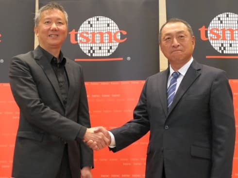
On October 24, 2023, TSMC, the leading Taiwanese semiconductor foundry, held a press conference in Tokyo to explain its Open Innovation Platform (OIP) ecosystem, TSMC 3DFabric Alliance for 3D packaging, and the standard specification "3Dblox" enabling the mutual use of tools and materials in the 3D packaging process. Ibiden, a major semiconductor package substrate manufacturer, also participated in the event, setting a goal to improve the productivity of semiconductor package substrates for advanced semiconductors by 10 times through the utilization of the OIP ecosystem and 3Dblox.

Dan Kochpatcharin from TSMC (left) and Koji Kawashima from Ibiden (right)
The conference took place alongside the "TSMC 2023 Japan OIP Ecosystem Forum," the first-ever event of its kind in Japan, attended by numerous domestic semiconductor industry stakeholders. Dan Kochpatcharin, the responsible department head of TSMC's Design Infrastructure Management Division, overseeing the operation of the OIP ecosystem, explained, "The OIP ecosystem, initiated by TSMC founder Morris Chang in 2008, aims to enhance the profitability of the semiconductor industry by sharing semiconductor technologies among various companies, including TSMC, from the early stages of development. With the OIP ecosystem, we can concurrently develop advanced processes and carry out the development and optimization of EDA tools and semiconductor IPs, shortening the time to mass production of semiconductor products by more than a year."
Furthermore, since its inception in 2008, the number of semiconductor IPs held by participating companies in the OIP ecosystem has increased from approximately 1,500 to over 70,000, a nearly 47-fold increase over the past 15 years. Kochpatcharin stated, "The effect of being able to proceed with the development of EDA tools and semiconductor IPs without waiting for the completion of advanced processes is evident in these numbers. In fact, while TSMC's 2nm process is still under development, EDA tools and semiconductor IPs from companies like Arm are already prepared and available."
However, the efforts of the OIP ecosystem were limited to the realm of semiconductor chip manufacturing. Recognizing the approaching limits of semiconductor miniaturization in 2022, TSMC launched the TSMC 3DFabric Alliance to further expand the OIP ecosystem for the advancement of 2.5D and 3D packaging, involving OSATs (Outsourced Semiconductor Assembly and Test), memory manufacturers, semiconductor package substrate manufacturers, and semiconductor tester vendors. The alliance aims to enable the mutual use of tools and materials for 2.5D/3D packaging through the standard specification, 3Dblox.
3Dblox, which was announced as version 1.0 at the end of 2022, is planned to be updated to version 1.5 in the summer of 2023 and version 2.0 by the end of 2023. Kochpatcharin emphasized, "AMD and Broadcom are already benefiting from 3Dblox, leading to early releases of semiconductor products with 3D packaging. Additionally, 3Dblox is an open specification that can be utilized by foundries that are our competitors."
Ibiden, a prominent semiconductor package substrate manufacturer, has been involved in the TSMC 3DFabric Alliance since its inception. Koji Kawashima, Executive Officer and Head of the Electronic Business Division at Ibiden, explained, "The technological trends in the semiconductor industry have greatly changed after the COVID-19 pandemic. Adoption of 2.5D and 3D packaging is expanding for further performance enhancements, and the size of semiconductor package substrates, which used to be around 40mm square, is now increasing to over 100mm square."
By leveraging the OIP ecosystem and 3Dblox, Ibiden will provide semiconductor manufacturers with technology files (Substrate Tech Files) related to semiconductor package substrates compliant with 3Dblox. Kawashima stated, "Until now, semiconductor package substrates have been individually designed for each semiconductor product, but as processes become more complex, the number of design revisions has increased. With the Substrate Tech File, it will be easier to accommodate various conditions such as substrate flatness, warpage, and materials. We will continue our efforts towards achieving a 10-fold increase in productivity compared to conventional methods through the utilization of the OIP ecosystem and 3Dblox."
▼▼▼
How Micron is Building the Biggest Chip Fab in U.S. History Despite a China Ban and Smartphone Slump
AMD China to Experience Massive Downsizing, Radeon Technology Group Affected The Most
Kioxia and Western Digital Merger This Month, Creating an Unbeatable Global Flash Memory Powerhouse
Israel Chip Maker Tower Makes Second Bid to Enter India with Fab Unit
Nokia to Axe up to 14,000 Jobs to Cut Costs
......
Read more latest news about the PCB and semiconductor industry here
+86 191 9627 2716
+86 181 7379 0595
8:30 a.m. to 5:30 p.m., Monday to Friday
