Samsung Electronics has decided to transition to a 200-layer NAND process at its NAND flash factory in Xi’an, China. The move to produce 236-layer products, which belong to the 8th generation of NAND, is seen as a strategic step to overcome a decline in performance due to sluggish global NAND demand.
According to industry sources on Oct. 15, Samsung’s executives have greenlit an upgrade to the NAND process in their Xi’an facility and have started extensive expansion efforts. Samsung has begun purchasing the latest semiconductor equipment for this transition, and new machinery is expected to be delivered by the end of the year.

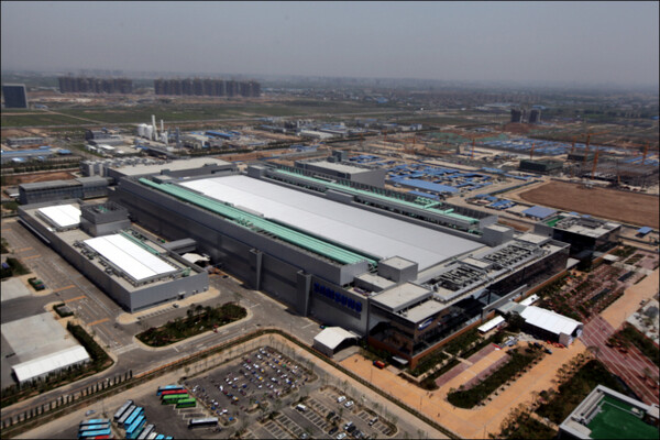
An aerial view of the Samsung semiconductor factory in Xi’an, China
The Xi’an factory of Samsung Electronics is the company’s only overseas memory semiconductor production base. Since its inception in 2014, the Xi’an facility expanded with a second factory in 2020 and has evolved into the world’s largest NAND manufacturing base, capable of producing 200,000 12-inch wafers per month. It accounts for over 40% of Samsung’s total NAND production. In this context, Samsung plans to sequentially introduce machinery in the Xi’an factory that can produce 236-layer (8th generation) NAND next year.
Samsung’s decision to upgrade its Xi’an factory is primarily due to two reasons. The first reason is to maintain its global leadership in the NAND market amid an environment where NAND flash market conditions are not showing signs of recovery. The IT market downturn and semiconductor market weakness, which began late last year, impacted Samsung’s NAND business, leading to increased unsold stock and subsequently widening losses.
Even after reducing production through a reduction policy, performance improvement was slow, prompting it to play the card of process upgrading. With the production of the latest 8th generation products, not only can it secure price competitiveness and demand, but considering that the 8th generation has more process steps than the 6th, wafer input can naturally be reduced by about 30%. This means there’s potential to balance market demand and supply.
In fact, Samsung officially declared a reduction in production in April. The operation rate of the Xi’an factory, which was the main production base for 6th generation (128-layer) V-NAND, also significantly decreased. Due to the limited market demand for legacy products (128-layer) and the inability to secure price competitiveness, it is known that the overall operation rate of the factory was reduced to the 20% range.
Another reason for the process shift is the temporary reprieve of Chinese semiconductor regulations by the U.S. for Samsung and SK hynix. Last October, the U.S. government required authorization for the sale of U.S.-made equipment to local chip production sites in China for the manufacturing of NAND flash above 128-layers, 14 nm or smaller, and DRAM 18 nm or smaller. As the U.S. government announced a “temporary” one-year export control reprieve for multinational semiconductor companies, including Samsung Electronics and SK hynix, concerns and anxieties grew among domestic semiconductor businesses about potential factory operation restrictions.
However, on Oct. 13 (local time), the U.S. Department of Commerce’s Bureau of Industry and Security (BIS) officially announced that the Chinese factories of Samsung Electronics and SK hynix will be exempt from the US’s regulations on semiconductor equipment against China. With this exemption regulation announcement by the U.S. government, the entry of local equipment for Samsung and SK has been permitted, allowing Samsung, which operates the NAND factory, to breathe a sigh of relief.
▼▼▼
Canon Challenges ASML with Innovative Technology for Chip Manufacturing
Chipmaker Qualcomm to lay off more than 1,200 staff in California
Israel-Hamas Conflict Threatens an Already-Vulnerable Chip Industry
Toshiba Acquired by JIP for $14 Billion, Set to Delist in Japan
Tsinghua University Unveils World's First Fully Integrated Memristor Chip
......
Read more latest news about the PCB and semiconductor industry here
+86 191 9627 2716
+86 181 7379 0595
8:30 a.m. to 5:30 p.m., Monday to Friday
